ZHCSKF4C March   2017  – October 2019 LMH1228

PRODUCTION DATA.  

  1. 特性
  2. 应用
  3. 说明
    1.     简化方框图
  4. 修订历史记录
  5. Pin Configuration and Functions
    1.     Pin Functions
  6. Specifications
    1. 6.1 Absolute Maximum Ratings
    2. 6.2 ESD Ratings
    3. 6.3 Recommended Operating Conditions
    4. 6.4 Thermal Information
    5. 6.5 Electrical Characteristics
    6. 6.6 Recommended SMBus Interface Timing Specifications
    7. 6.7 Serial Parallel Interface (SPI) Timing Specifications
    8. 6.8 Typical Characteristics
  7. Detailed Description
    1. 7.1 Overview
    2. 7.2 Functional Block Diagram
    3. 7.3 Feature Description
      1. 7.3.1 4-Level Input Pins and Thresholds
      2. 7.3.2 OUT0_SEL and SDI_OUT2_SEL Control
      3. 7.3.3 Input Signal Detect
      4. 7.3.4 Continuous Time Linear Equalizer (CTLE)
      5. 7.3.5 Clock and Data (CDR) Recovery
      6. 7.3.6 Internal Eye Opening Monitor (EOM)
      7. 7.3.7 Output Function Control
      8. 7.3.8 Output Driver Control
        1. 7.3.8.1 Line-Side Output Cable Driver (SDI_OUT1+, SDI_OUT2+)
          1. 7.3.8.1.1 Output Amplitude (VOD)
          2. 7.3.8.1.2 Output Pre-Emphasis
          3. 7.3.8.1.3 Output Slew Rate
          4. 7.3.8.1.4 Output Polarity Inversion
        2. 7.3.8.2 Host-Side 100-Ω Output Driver (OUT0±)
      9. 7.3.9 Status Indicators and Interrupts
        1. 7.3.9.1 LOCK_N (Lock Indicator)
        2. 7.3.9.2 SD_N (Signal Detect)
        3. 7.3.9.3 INT_N (Interrupt)
    4. 7.4 Device Functional Modes
      1. 7.4.1 System Management Bus (SMBus) Mode
        1. 7.4.1.1 SMBus Read and Write Transaction
          1. 7.4.1.1.1 SMBus Write Operation Format
          2. 7.4.1.1.2 SMBus Read Operation Format
      2. 7.4.2 Serial Peripheral Interface (SPI) Mode
        1. 7.4.2.1 SPI Read and Write Transactions
        2. 7.4.2.2 SPI Write Transaction Format
        3. 7.4.2.3 SPI Read Transaction Format
        4. 7.4.2.4 SPI Daisy Chain
    5. 7.5 Register Maps
  8. Application and Implementation
    1. 8.1 Application Information
      1. 8.1.1 SMPTE Requirements and Specifications
      2. 8.1.2 Low-Power Optimization
      3. 8.1.3 Optimized Loop Bandwidth Settings for Arria 10 FPGA Applications
    2. 8.2 Typical Applications
      1. 8.2.1 Dual Cable Driver
        1. 8.2.1.1 Design Requirements
        2. 8.2.1.2 Detailed Design Procedure
        3. 8.2.1.3 Application Curves
      2. 8.2.2 Distribution Amplifier
        1. 8.2.2.1 Design Requirements
        2. 8.2.2.2 Detailed Design Procedure
        3. 8.2.2.3 Application Curves
  9. Power Supply Recommendations
  10. 10Layout
    1. 10.1 Layout Guidelines
      1. 10.1.1 Board Stack-Up and Ground References
      2. 10.1.2 High-Speed PCB Trace Routing and Coupling
        1. 10.1.2.1 SDI_OUT1± and SDI_OUT2±:
        2. 10.1.2.2 IN0± and OUT0±:
      3. 10.1.3 Anti-Pads
      4. 10.1.4 BNC Connector Layout and Routing
      5. 10.1.5 Power Supply and Ground Connections
      6. 10.1.6 Footprint Recommendations
    2. 10.2 Layout Example
  11. 11器件和文档支持
    1. 11.1 文档支持
      1. 11.1.1 相关文档
    2. 11.2 接收文档更新通知
    3. 11.3 支持资源
    4. 11.4 商标
    5. 11.5 静电放电警告
    6. 11.6 出口管制提示
    7. 11.7 Glossary
  12. 12机械、封装和可订购信息
    1. 12.1 Package Option Addendum
      1. 12.1.1 Packaging Information
      2. 12.1.2 Tape and Reel Information

封装选项

机械数据 (封装 | 引脚)
散热焊盘机械数据 (封装 | 引脚)
订购信息

Application Curves

The LMH1228 performance on OUT0± was measured with the test setup shown in Figure 22.

LMH1228 app_test_setup_diagram_OUT0.gifFigure 35. Test Setup for LMH1228 to OUT0±

The eye diagrams in this subsection show how the LMH1228 improves overall signal integrity in the data path for 100-Ω differential FR4 PCB trace at IN0±.
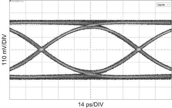
LMH1228 CD_OUT0_11.88_PRBS10_110mV_14ps.png
Measured at OUT0±
HOST_EQ0 = F, SDI_OUT2_SEL = L, OUT_CTRL = F
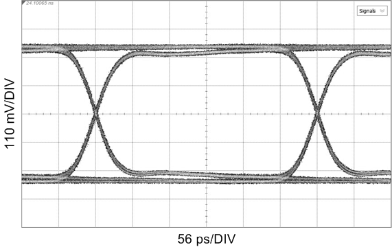
Figure 36. 11.88 Gbps, TL = 20" FR4, Reclocked
LMH1228 CD_OUT0_2.97_PRBS10_110mV_56ps.png
Measured at OUT0±
HOST_EQ0 = F, SDI_OUT2_SEL = L, OUT_CTRL = F
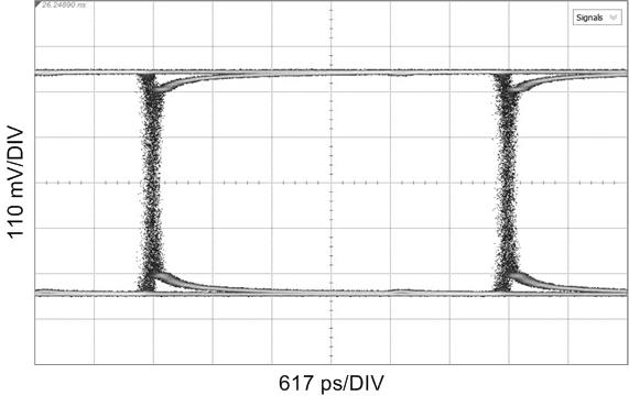
Figure 38. 2.97 Gbps, TL = 20" FR4, Reclocked
LMH1228 CD_OUT0_270M_PRBS10_110mV_617ps.png
Measured at OUT0±
HOST_EQ0 = F, SDI_OUT2_SEL = L, OUT_CTRL = F
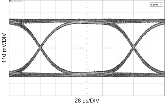
Figure 40. 270 Mbps, TL = 20" FR4, Reclocked
LMH1228 CD_OUT0_5.94_PRBS10_110mV_28ps.png
Measured at OUT0±
HOST_EQ0 = F, SDI_OUT2_SEL = L, OUT_CTRL = F
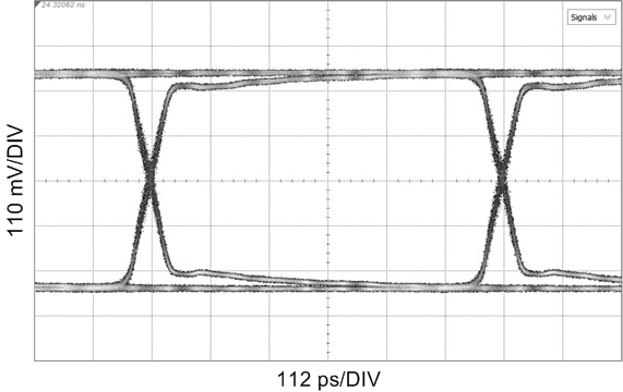
Figure 37. 5.94 Gbps, TL = 20" FR4, Reclocked
LMH1228 CD_OUT0_1.485_PRBS10_110mV_112ps.png
Measured at OUT0±
HOST_EQ0 = F, SDI_OUT2_SEL = L, OUT_CTRL = F
Figure 39. 1.485 Gbps, TL = 20" FR4, Reclocked