ZHCS547K January 2010 – February 2018 LM27402
PRODUCTION DATA.
- 1 特性
- 2 应用
- 3 说明
- 4 修订历史记录
- 5 Pin Configuration and Functions
- 6 Specifications
-
7 Detailed Description
- 7.1 Overview
- 7.2 Functional Block Diagram
- 7.3
Feature Description
- 7.3.1 Wide Input Voltage Range
- 7.3.2 UVLO
- 7.3.3 Precision Enable
- 7.3.4 Soft-Start and Voltage Tracking
- 7.3.5 Output Voltage Setpoint and Accuracy
- 7.3.6 Voltage-Mode Control
- 7.3.7 Power Good
- 7.3.8 Inductor-DCR-Based Overcurrent Protection
- 7.3.9 Current Sensing
- 7.3.10 Power MOSFET Gate Drivers
- 7.3.11 Pre-Bias Start-up
- 7.4 Device Functional Modes
-
8 Application and Implementation
- 8.1
Application Information
- 8.1.1 Converter Design
- 8.1.2 Inductor Selection (L)
- 8.1.3 Output Capacitor Selection (COUT)
- 8.1.4 Input Capacitor Selection (CIN)
- 8.1.5 Using Precision Enable
- 8.1.6 Setting the Soft-Start Time
- 8.1.7 Tracking
- 8.1.8 Setting the Switching Frequency
- 8.1.9 Setting the Current Limit Threshold
- 8.1.10 Control Loop Compensation
- 8.1.11 MOSFET Gate Drivers
- 8.1.12 Power Loss and Efficiency Calculations
- 8.2 Typical Applications
- 8.1
Application Information
- 9 Power Supply Recommendations
- 10Layout
- 11器件和文档支持
- 12机械、封装和可订购信息
封装选项
机械数据 (封装 | 引脚)
散热焊盘机械数据 (封装 | 引脚)
订购信息
7.3.9 Current Sensing
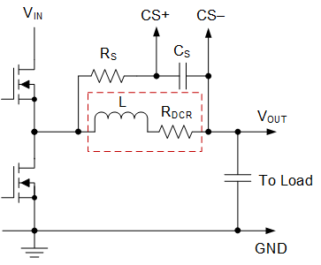
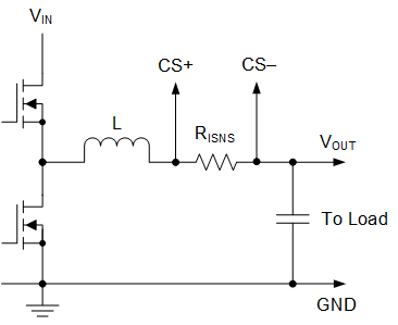
As mentioned, the LM27402 implements a lossless inductor DCR lossless current sense scheme designed to provide both accurate overload (current limit) and short-circuit protection. Figure 22 shows the popular inductor DCR current sense method. Figure 23 shows an implementation with current shunt resistor, RISNS.
Components RS and CS in Figure 22 create a low-pass filter across the inductor to enable differential sensing of the inductor DCR voltage drop. When RSCS is equal to L/RDCR, the voltage developed across the sense capacitor, CS, is a replica of the voltage waveform of the inductor DCR. Choose the capacitance of CS greater than 0.1 µF to maintain low impedance of the sense network, thus reducing the susceptibility of noise pickup from the switch node.
 Figure 22. Current Sensing Using Inductor DCR
 Figure 23. Current Sensing Using Shunt Resistor
Note that the inductor DCR is shown schematically as a discrete element in Figure 22. With power inductors selected to provide lowest possible DCR to minimize power losses, the typical DCR ranges from 0.4 mΩ to
4 mΩ. Then, given a load current of 25 A, the voltage presented across the CS+ and CS– pins ranges between 10 mV and 100 mV.
A current sense (or current shunt) resistor in series with the inductor can also be implemented at lower output current levels to provide accurate overcurrent protection, see Figure 23. Burdened by the unavoidable efficiency penalty and/or additional cost implications, this configuration is not usually implemented in high-current applications (except where OCP setpoint accuracy and stability over the operating temperature range are critical specifications).