ZHCS547K January 2010 – February 2018 LM27402
PRODUCTION DATA.
- 1 特性
- 2 应用
- 3 说明
- 4 修订历史记录
- 5 Pin Configuration and Functions
- 6 Specifications
-
7 Detailed Description
- 7.1 Overview
- 7.2 Functional Block Diagram
- 7.3
Feature Description
- 7.3.1 Wide Input Voltage Range
- 7.3.2 UVLO
- 7.3.3 Precision Enable
- 7.3.4 Soft-Start and Voltage Tracking
- 7.3.5 Output Voltage Setpoint and Accuracy
- 7.3.6 Voltage-Mode Control
- 7.3.7 Power Good
- 7.3.8 Inductor-DCR-Based Overcurrent Protection
- 7.3.9 Current Sensing
- 7.3.10 Power MOSFET Gate Drivers
- 7.3.11 Pre-Bias Start-up
- 7.4 Device Functional Modes
-
8 Application and Implementation
- 8.1
Application Information
- 8.1.1 Converter Design
- 8.1.2 Inductor Selection (L)
- 8.1.3 Output Capacitor Selection (COUT)
- 8.1.4 Input Capacitor Selection (CIN)
- 8.1.5 Using Precision Enable
- 8.1.6 Setting the Soft-Start Time
- 8.1.7 Tracking
- 8.1.8 Setting the Switching Frequency
- 8.1.9 Setting the Current Limit Threshold
- 8.1.10 Control Loop Compensation
- 8.1.11 MOSFET Gate Drivers
- 8.1.12 Power Loss and Efficiency Calculations
- 8.2 Typical Applications
- 8.1
Application Information
- 9 Power Supply Recommendations
- 10Layout
- 11器件和文档支持
- 12机械、封装和可订购信息
封装选项
机械数据 (封装 | 引脚)
散热焊盘机械数据 (封装 | 引脚)
订购信息
6.8 Typical Performance Characteristics
Unless otherwise stated, all data sheet curves were recorded using Example Circuit 1. VIN = 12 V.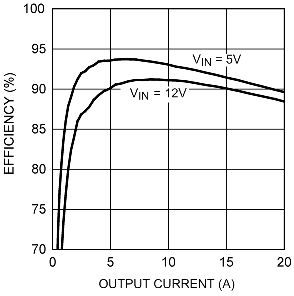 Figure 1. Efficiency (Vout = 1.5 V)
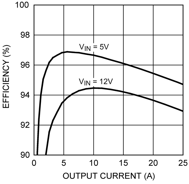 Figure 3. Efficiency (Vout = 3.3 V, Example Circuit 2)
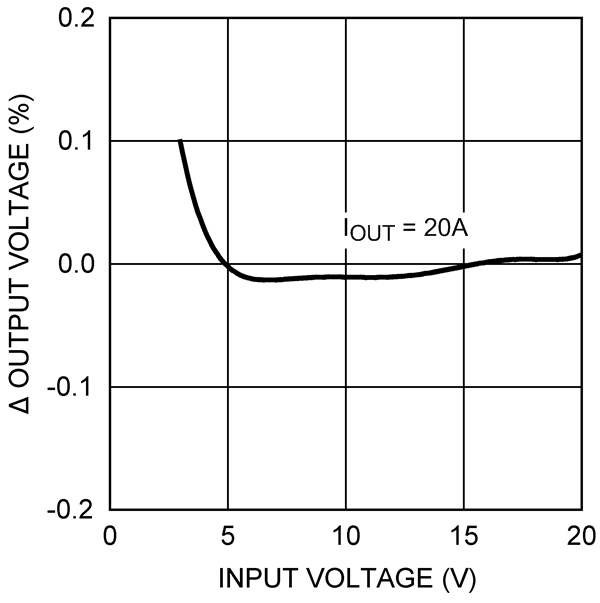 Figure 5. Line Regulation (Vout = 1.5 V)
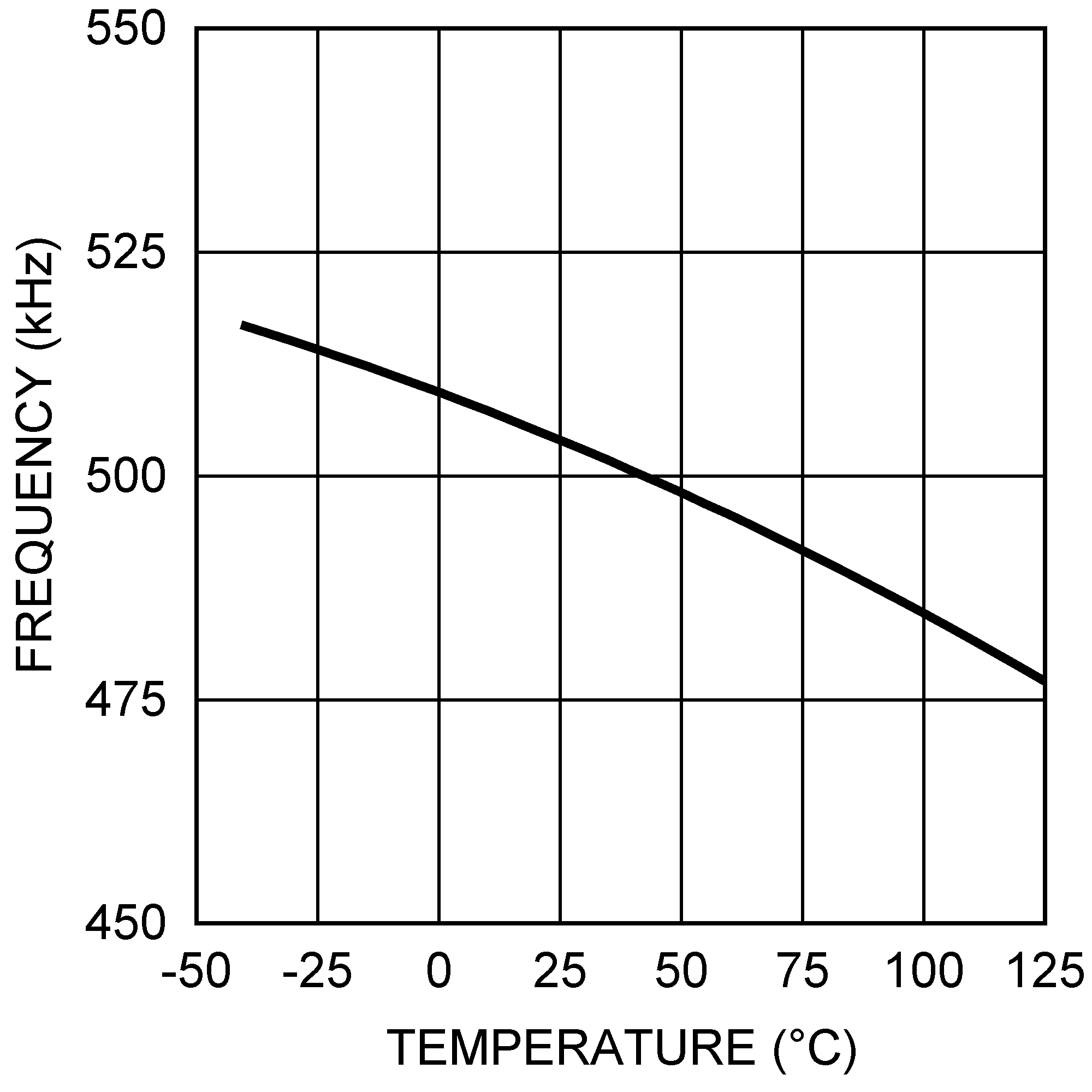 Figure 7. Frequency vs Temperature (RFADJ = 20 kΩ)
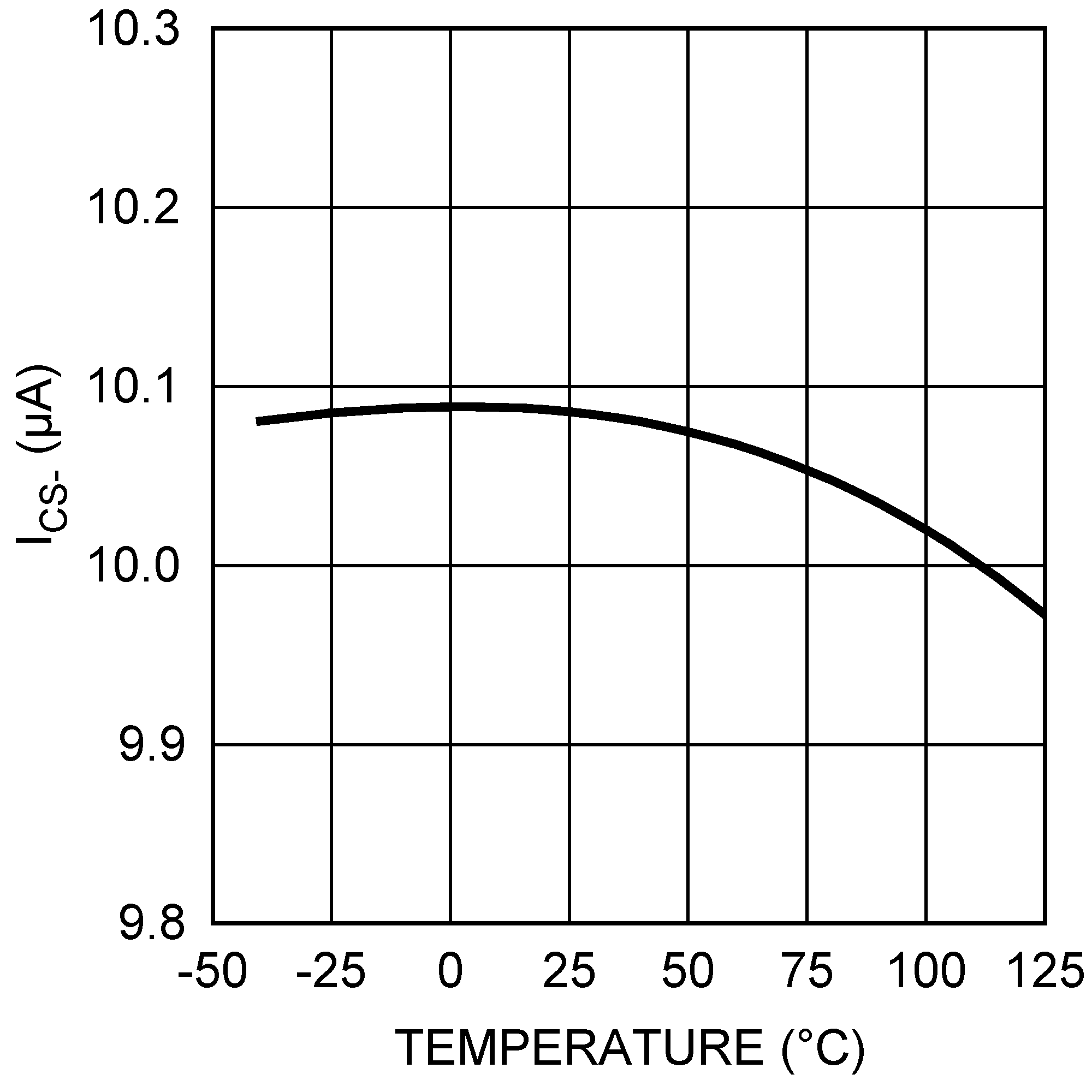 Figure 9. CS– Current Source vs Temperature
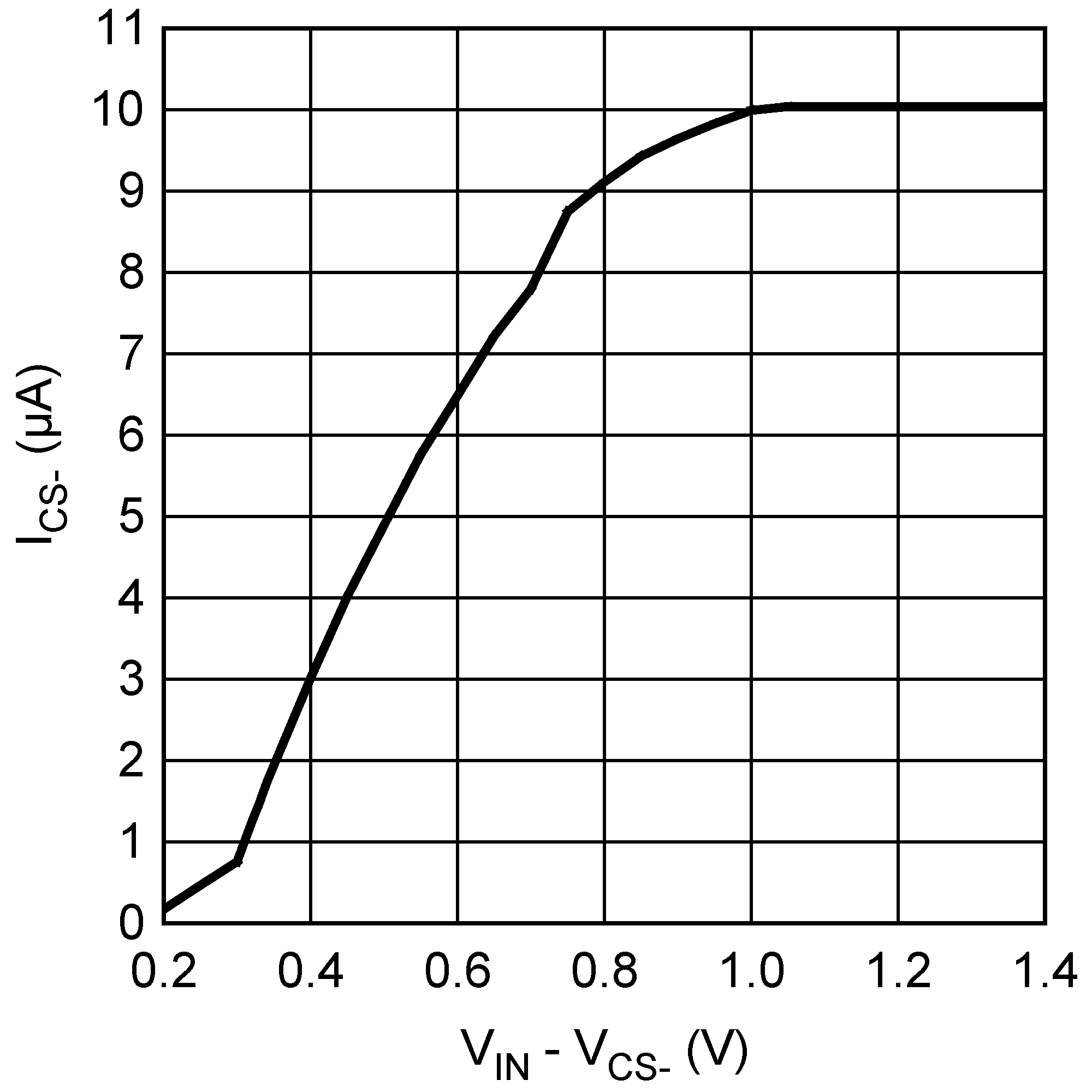 Figure 11. CS– Current Source Compliance Voltage
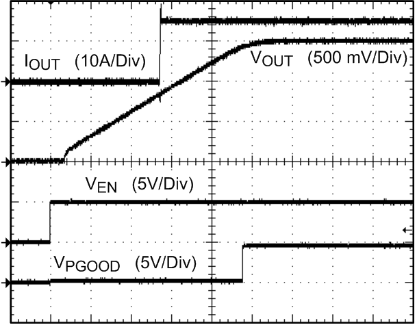
Horizontal Scale: 2 ms/DIV
Figure 13. Start-up Waveforms
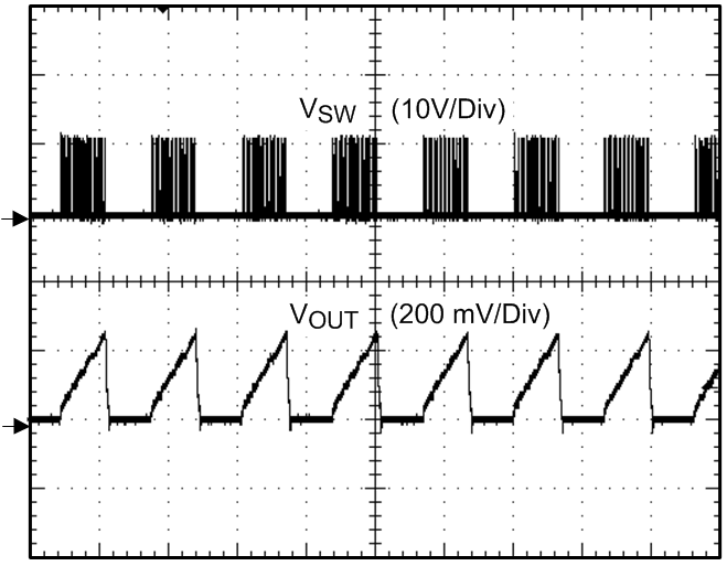
Horizontal Scale: 2 ms/DIV
Figure 15. OCP Hiccup
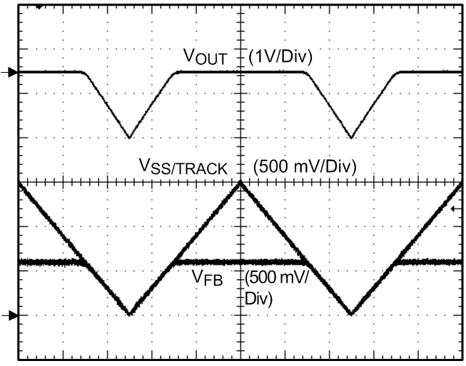
Horizontal Scale: 2 ms/DIV
Figure 17. Tracking
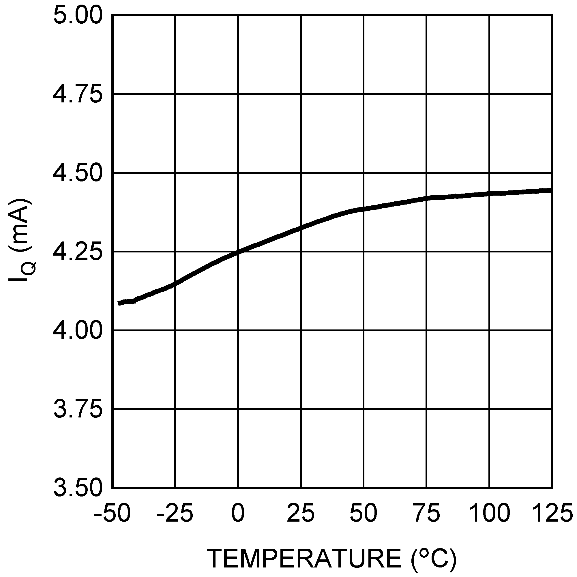 Figure 19. Quiescent Current vs Temperature
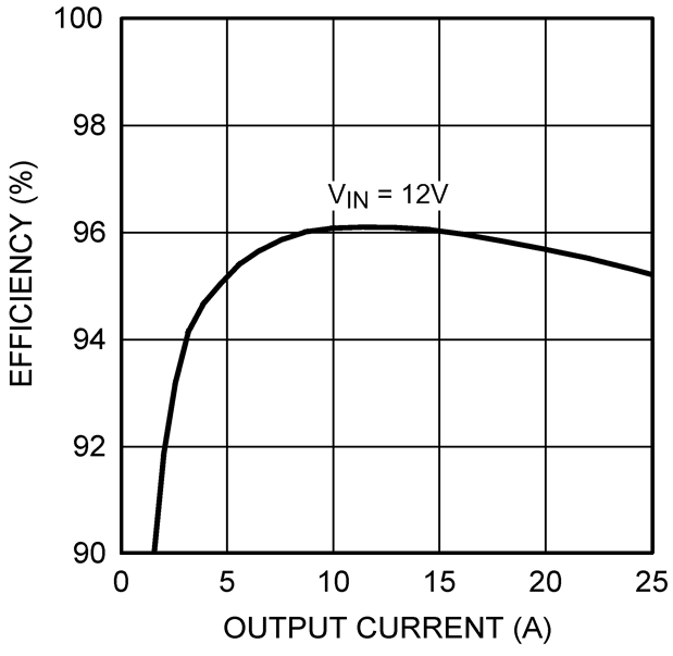 Figure 2. Efficiency (Vout = 5 V, Example Circuit 2)
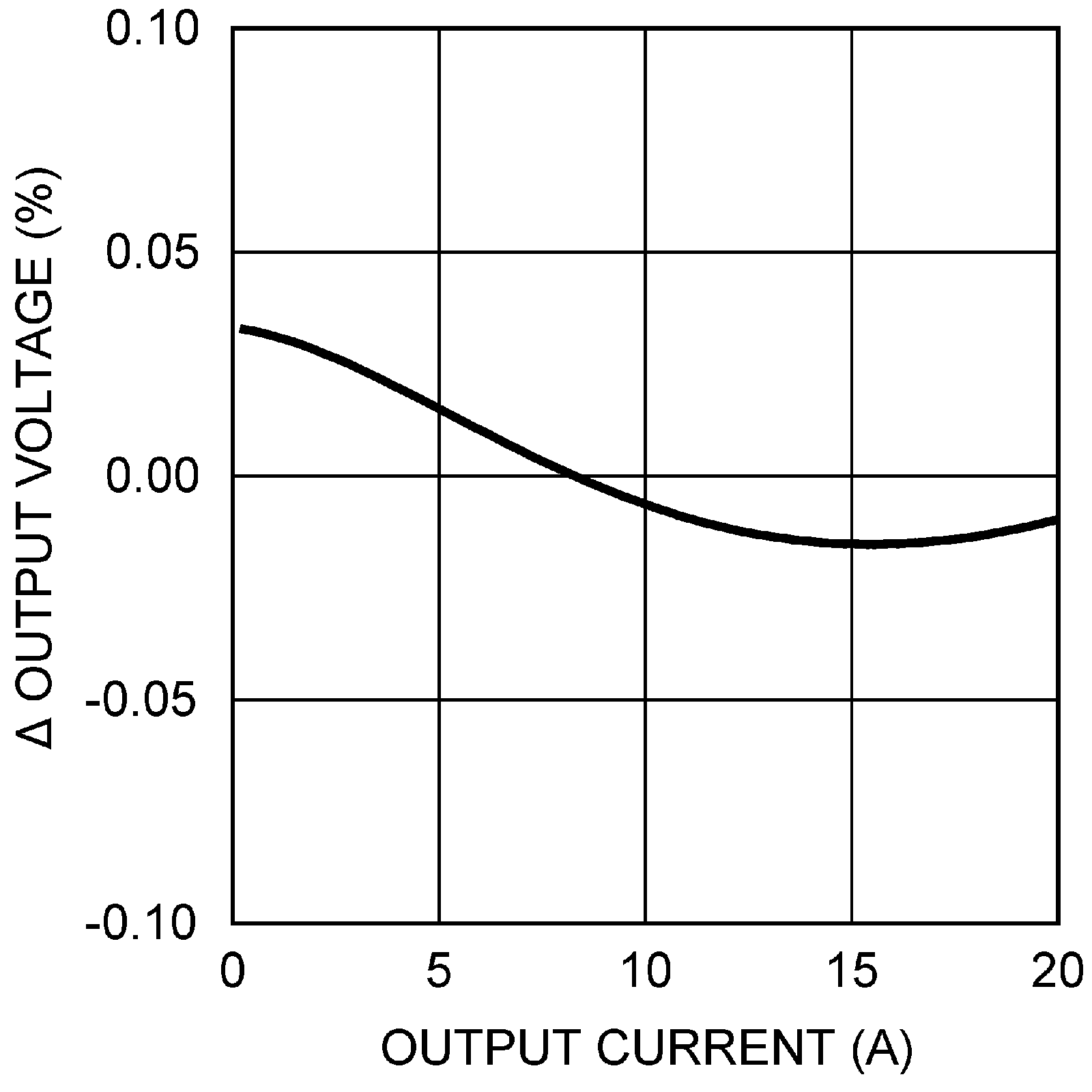 Figure 4. Load Regulation (Vout = 1.5 V)
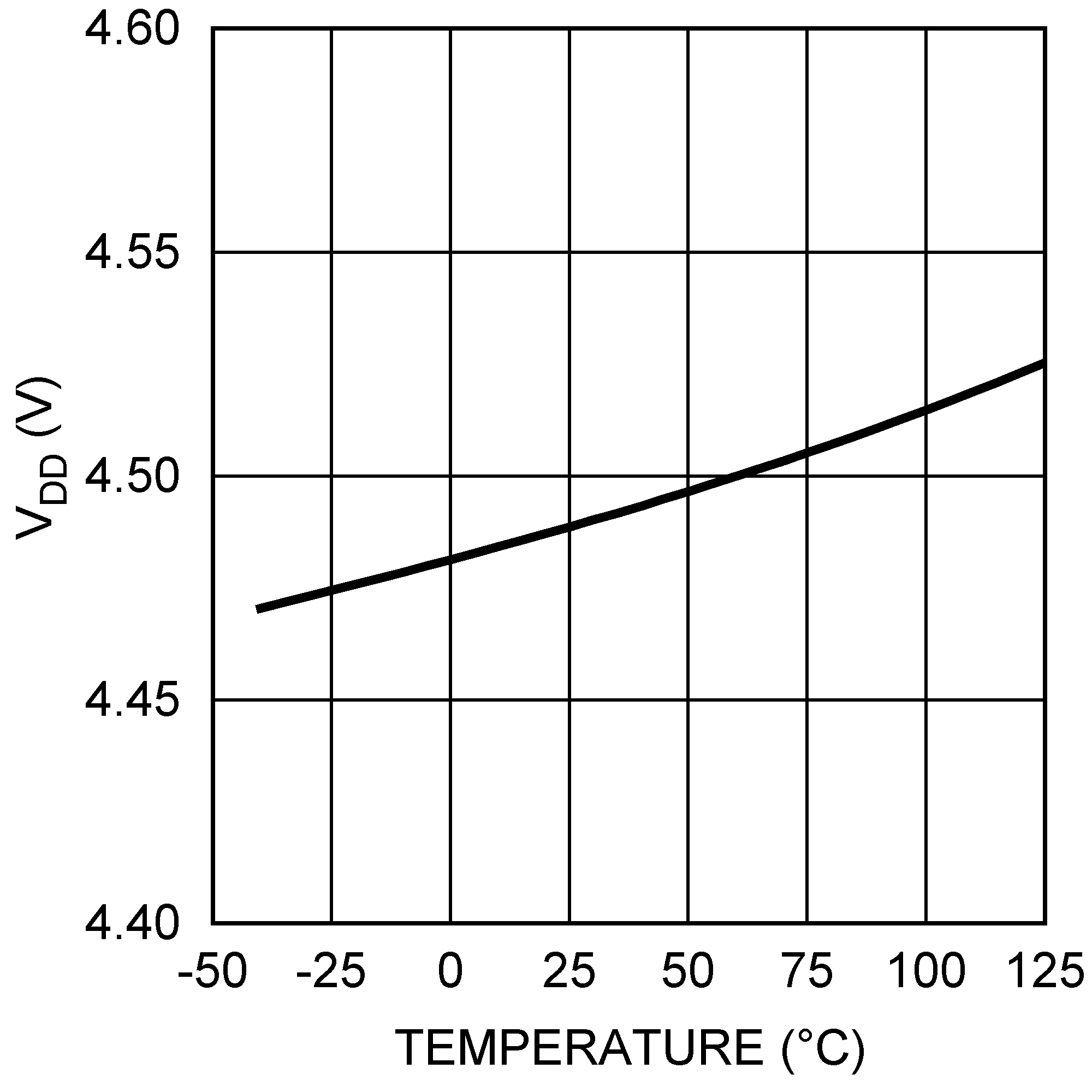 Figure 6. VDD Voltage vs Temperature (IVDD = 25 mA)
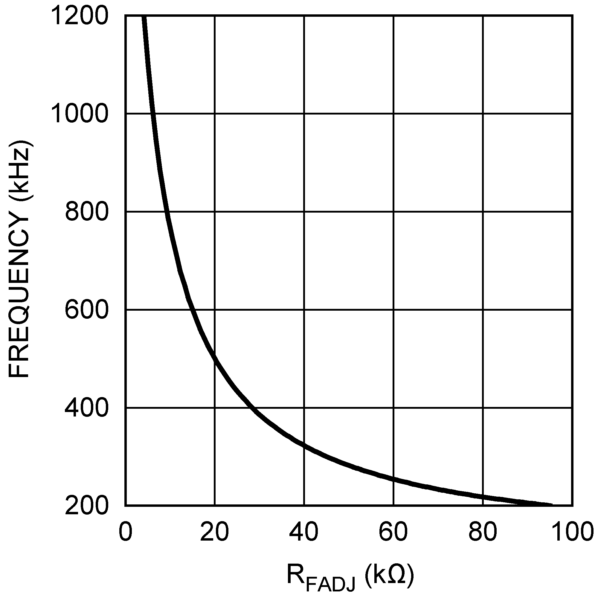 Figure 8. Frequency vs RFADJ
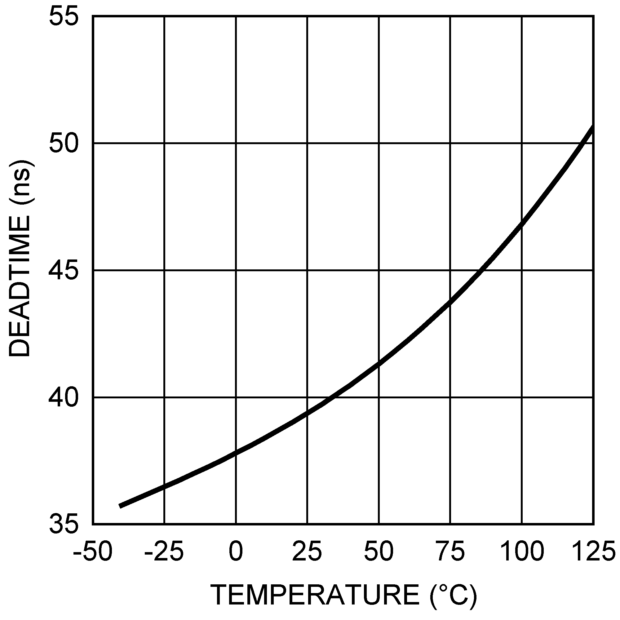 Figure 10. Deadtime vs Temperature
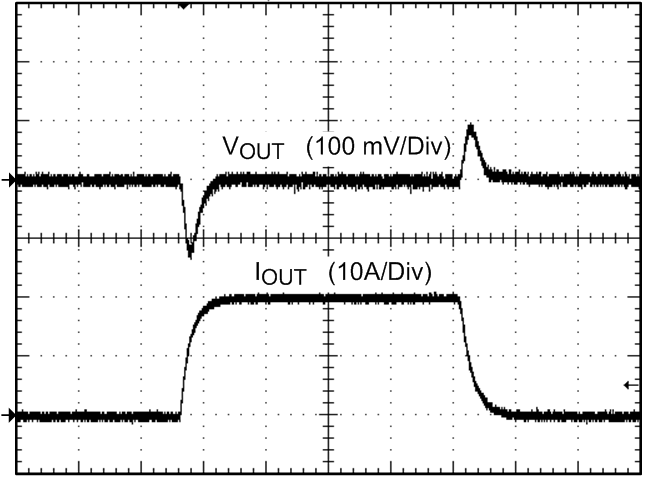
Horizontal Scale: 100 µs/DIV
Figure 12. Load Transient
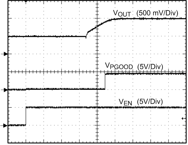
Horizontal Scale: 2 ms/DIV
Figure 14. Pre-Bias Start-up
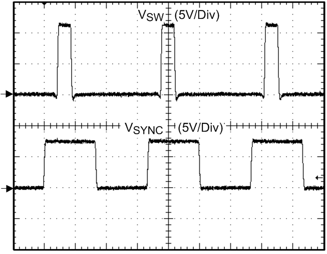
Horizontal Scale: 400 ns/DIV
Figure 16. Frequency Synchronization
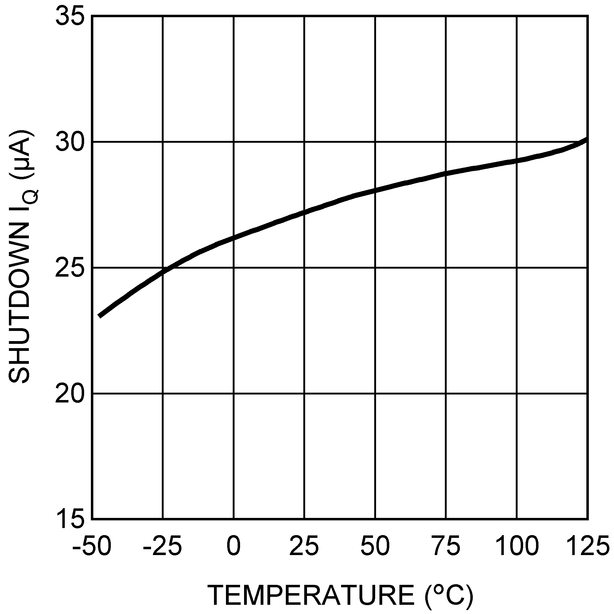 Figure 18. Shutdown Quiescent Current vs Temperature
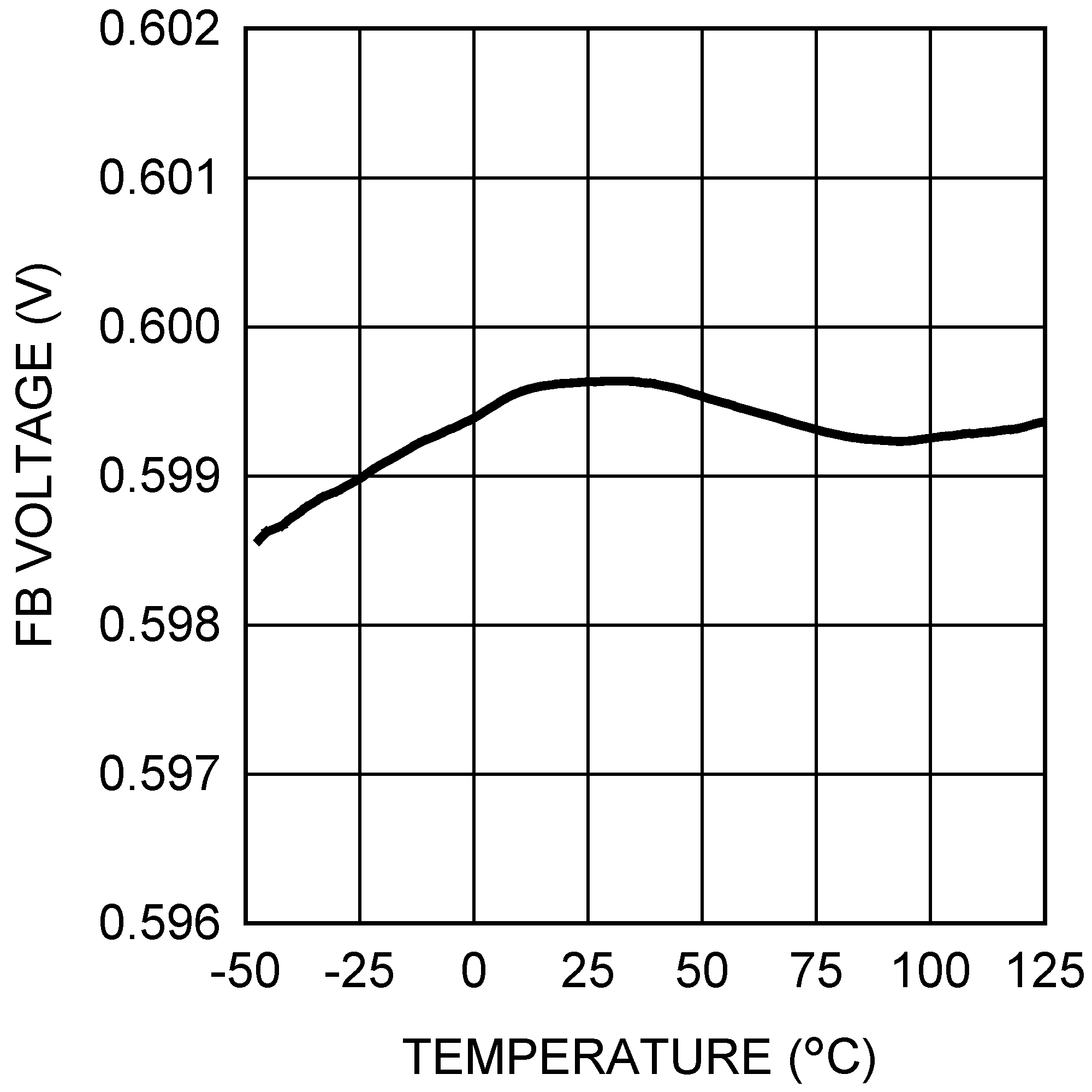 Figure 20. Feedback Voltage vs Temperature