ZHCSNV5 October   2021 LM117HVQML-SP

PRODUCTION DATA  

  1. 特性
  2. 应用
  3. 说明
  4. Revision History
  5. Related Products
  6. Pin Configurations and Functions
  7. Specifications
    1. 7.1 Absolute Maximum Ratings
    2. 7.2 ESD Ratings
    3. 7.3 Recommended Operating Conditions
    4. 7.4 Thermal Information
    5. 7.5 Electrical Characteristics
    6. 7.6 Parameter Drift
    7. 7.7 Quality Conformance Inspection
    8. 7.8 Typical Characteristics
  8. Detailed Description
    1. 8.1 Overview
    2. 8.2 Functional Block Diagram
      1. 8.2.1 Simplified Device Schematic
    3. 8.3 Feature Description
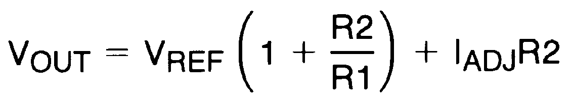
      1. 8.3.1 Setting Output Voltage
      2. 8.3.2 Load Regulation
      3. 8.3.3 External Capacitors
      4. 8.3.4 Protection Diodes
  9. Application and Implementation
    1. 9.1 Typical Applications
  10. 10Power Supply Recommendations
  11. 11Layout
    1. 11.1 Layout Guidelines
  12. 12Device and Documentation Support
    1. 12.1 Device Support
      1. 12.1.1 第三方产品免责声明
    2. 12.2 Documentation Support
      1. 12.2.1 Related Documentation
    3. 12.3 接收文档更新通知
    4. 12.4 支持资源
    5. 12.5 Trademarks
    6. 12.6 Electrostatic Discharge Caution
    7. 12.7 术语表
  13. 13Mechanical, Packaging, and Orderable Information

封装选项

机械数据 (封装 | 引脚)
散热焊盘机械数据 (封装 | 引脚)
订购信息

Setting Output Voltage

In operation, the LM117HVQML-SP develops a nominal 1.25-V reference voltage, VREF, between the output and adjustment terminal. The reference voltage is expressed across R1 and, since the voltage is constant, a constant current I1 then flows through R2, giving an output voltage of:

Equation 1. GUID-EE18A2FF-B4D4-49AD-8BBD-C51773FDFAF5-low.png
GUID-2C1AF196-3D71-454F-92A1-DD400E64E321-low.png

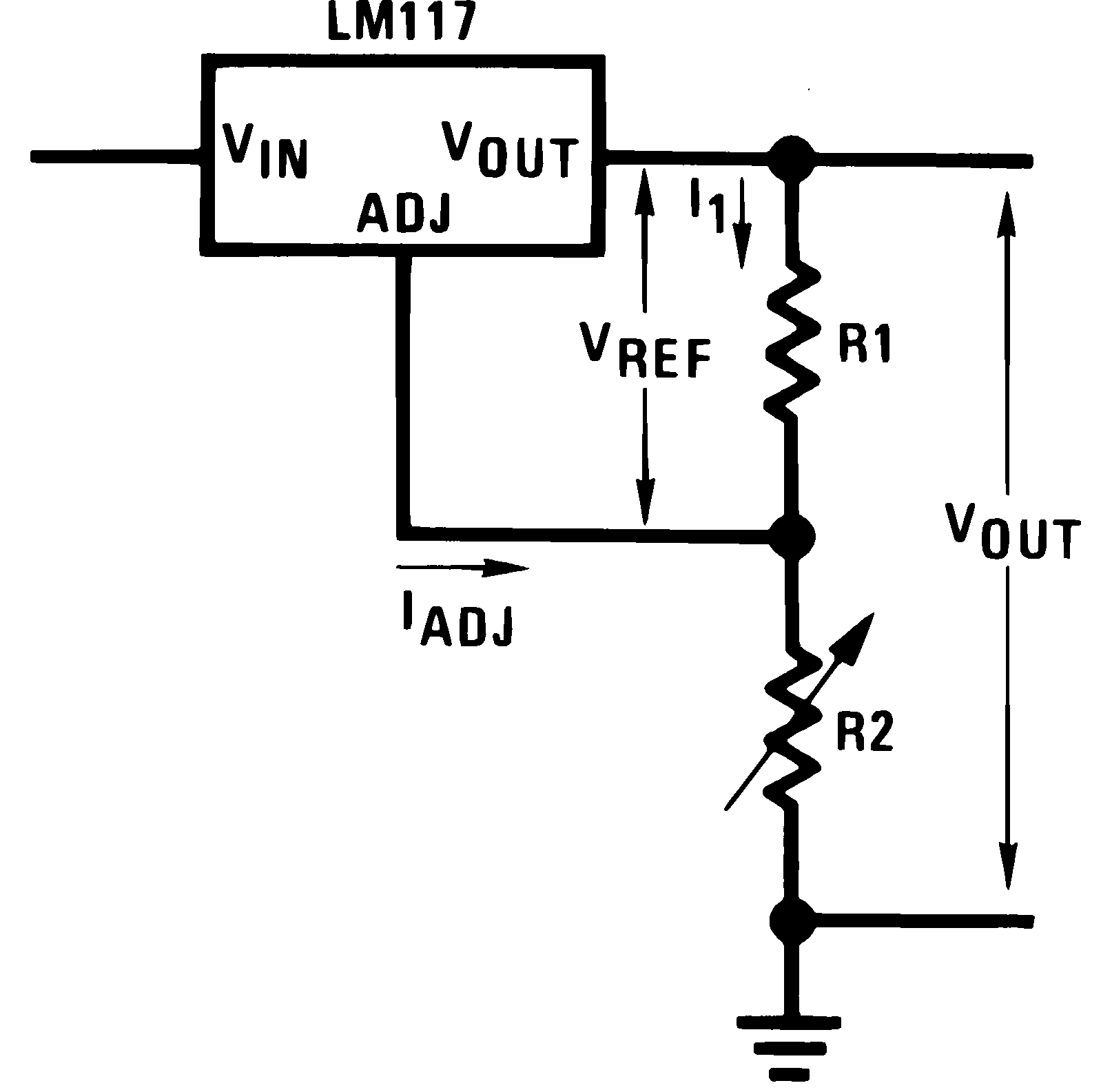
Since the 100-μA current from the adjustment terminal represents an error term, the LM117HVQML-SP was designed to minimize IADJ and make it very constant with line and load changes. To do this, all quiescent operating current is returned to the output establishing a minimum load current requirement. If there is insufficient load on the output, the output will rise.

To mitigate the requirement for an added load to sink the required output current, the resistor divider may be selected so that it alone can sink the largest specified output load current of 5 mA (nominal). This has the additional benefit of minimizing the IADJ error term (which varies over temperature).