ZHCSC07E December 2013 – March 2019 DLPC2607
PRODUCTION DATA.
- 1 特性
- 2 应用范围
- 3 说明
- 4 修订历史记录
- 5 Pin Configuration and Functions
-
6 Specifications
- 6.1 Absolute Maximum Ratings
- 6.2 ESD Ratings
- 6.3 Recommended Operating Conditions
- 6.4 Thermal Information
- 6.5 Typical Current and Power Dissipation
- 6.6 I/O Characteristics
- 6.7 Internal Pullup and Pulldown Characteristics
- 6.8 Parallel I/F Frame Timing Requirements
- 6.9 Parallel I/F General Timing Requirements
- 6.10 Parallel I/F Maximum Parallel Interface Horizontal Line Rate
- 6.11 BT.656 I/F General Timing Requirements
- 6.12 100- to 120-Hz Operational Limitations
- 6.13 Flash Interface Timing Requirements
- 6.14 DMD Interface Timing Requirements
- 6.15 mDDR Memory Interface Timing Requirements
- 7 Detailed Description
- 8 Application and Implementation
- 9 Power Supply Recommendations
-
10Layout
- 10.1
Layout Guidelines
- 10.1.1 Internal ASIC PLL Power
- 10.1.2 General Handling Guidelines for Unused CMOS-Type Pins
- 10.1.3 SPI Signal Routing
- 10.1.4 mDDR Memory and DMD Interface Considerations
- 10.1.5 PCB Design
- 10.1.6 General PCB Routing (Applies to All Corresponding PCB Signals)
- 10.1.7 Maximum, Pin-to-Pin, PCB Interconnects Etch Lengths
- 10.1.8 I/F Specific PCB Routing
- 10.1.9 Number of Layer Changes
- 10.1.10 Stubs
- 10.1.11 Termination Requirements:
- 10.2 Layout Example
- 10.1
Layout Guidelines
- 11器件和文档支持
- 12机械、封装和可订购信息
请参考 PDF 数据表获取器件具体的封装图。
机械数据 (封装 | 引脚)
- ZVB|176
散热焊盘机械数据 (封装 | 引脚)
8.2.4 Application Curve
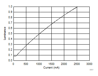
As the LED currents that are driven time-sequentially through the red, green, and blue LEDs are increased, the brightness of the projector increases. This increase is somewhat non-linear, and the curve for typical white screen lumens changes with LED currents is shown in Figure 12. For the LED currents shown, it is assumed that the same current amplitude is applied to the red, green, and blue LEDs.
 Figure 12. Luminance vs Current
 As with prior DLP electronics solutions, image data is 100% digital from the DLPC2607 device input port to the image projected on to the display screen. The image stays in digital form and is never converted into an analog signal. The DLPC2607 device processes the digital input image and converts the data into bit-plane format as needed by the DMD. The DMD then reflects light to the screen using binary pulse-width modulation (PWM) for each pixel mirror. The viewer’s eyes integrate this light to form brilliant, crisp images.