ZHCSGZ7E March 2017 – May 2021 CC3220MOD , CC3220MODA
PRODUCTION DATA
- 1 特性
- 2 应用
- 3 说明
- 4 功能方框图
- 5 Revision History
- 6 Device Comparison
- 7 Terminal Configuration and Functions
-
8 Specifications
- 8.1 Absolute Maximum Ratings
- 8.2 ESD Ratings
- 8.3 Recommended Operating Conditions
- 8.4 Current Consumption (CC3220MODS and CC3220MODAS)
- 8.5 Current Consumption (CC3220MODSF and CC3220MODASF)
- 8.6 TX Power and IBAT Versus TX Power Level Settings
- 8.7 Brownout and Blackout Conditions
- 8.8 Electrical Characteristics
- 8.9 CC3220MODAx Antenna Characteristics
- 8.10 WLAN Receiver Characteristics
- 8.11 WLAN Transmitter Characteristics
- 8.12 Reset Requirement
- 8.13 Thermal Resistance Characteristics for MOB and MON Packages
- 8.14
Timing and Switching Characteristics
- 8.14.1 Power-Up Sequencing
- 8.14.2 Power-Down Sequencing
- 8.14.3 Device Reset
- 8.14.4 Wake Up From Hibernate Timing
- 8.14.5 Peripherals Timing
-
9 Detailed Description
- 9.1 Overview
- 9.2 Arm® Cortex®-M4 处理器内核子系统
- 9.3 Wi-Fi® Network Processor Subsystem
- 9.4 Security
- 9.5 Power-Management Subsystem
- 9.6 Low-Power Operating Mode
- 9.7 Memory
- 9.8 Restoring Factory Default Configuration
- 9.9 Boot Modes
- 9.10 Device Certification and Qualification
- 9.11 Module Markings
- 9.12 End Product Labeling
- 9.13 Manual Information to the End User
- 10Applications, Implementation, and Layout
- 11Environmental Requirements and Specifications
- 12Device and Documentation Support
- 13Mechanical, Packaging, and Orderable Information
请参考 PDF 数据表获取器件具体的封装图。
机械数据 (封装 | 引脚)
- MON|63
散热焊盘机械数据 (封装 | 引脚)
8.14.4 Wake Up From Hibernate Timing
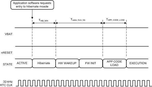
Table 8-3 lists the software hibernate timing requirements.
Note:
The internal 32.768-kHz crystal is kept enabled by default when the module goes to hibernate.
Table 8-3 Software Hibernate Timing
Requirements
| ITEM | NAME | DESCRIPTION | MIN | TYP | MAX | UNIT |
|---|---|---|---|---|---|---|
| THIB_MIN | Minimum hibernate time | 10 | ms | |||
| Twake_from_hib(1) | Hardware wakeup time plus firmware initialization time | 50(2) | ms | |||
| T_APP_CODE_LOAD | App code load time for CC3220MODS and CC3220MODAS | CC3220MODS and CC3220MODAS | Image size (KB) × 1.7 ms | |||
| App code load time for CC3220MODSF and CC3220MODASF | CC3220MODSF and CC3220MODASF | Image size (KB) × 0.06 ms | ||||
(1) Twake_from_hib can be 200 ms on rare occasions when
calibration is performed. Calibration is performed sparingly, typically when
exiting Hibernate and only if temperature has changed by more than 20°C or more
than 24 hours have elapsed since a prior calibration.
(2) Wake-up time can extend to 75 ms if a patch is downloaded from
the serial Flash.
Figure 8-7 shows the timing diagram for wake up from the hibernate state.
 Figure 8-7 Wake Up From Hibernate Timing
Diagram