ZHCSGZ7E March   2017  – May 2021 CC3220MOD , CC3220MODA

PRODUCTION DATA  

  1. 特性
  2. 应用
  3. 说明
  4. 功能方框图
  5. Revision History
  6. Device Comparison
    1. 6.1 Related Products
  7. Terminal Configuration and Functions
    1. 7.1 CC3220MODx and CC3220MODAx Pin Diagram
    2. 7.2 Pin Attributes
      1. 7.2.1 Module Pin Attributes
    3. 7.3 Connections for Unused Pins
    4. 7.4 Pin Attributes and Pin Multiplexing
    5. 7.5 Drive Strength and Reset States for Analog-Digital Multiplexed Pins
    6. 7.6 Pad State After Application of Power to Chip, but Before Reset Release
  8. Specifications
    1. 8.1  Absolute Maximum Ratings
    2. 8.2  ESD Ratings
    3. 8.3  Recommended Operating Conditions
    4. 8.4  Current Consumption (CC3220MODS and CC3220MODAS)
    5. 8.5  Current Consumption (CC3220MODSF and CC3220MODASF)
    6. 8.6  TX Power and IBAT Versus TX Power Level Settings
    7. 8.7  Brownout and Blackout Conditions
    8. 8.8  Electrical Characteristics
    9. 8.9  CC3220MODAx Antenna Characteristics
    10. 8.10 WLAN Receiver Characteristics
    11. 8.11 WLAN Transmitter Characteristics
    12. 8.12 Reset Requirement
    13. 8.13 Thermal Resistance Characteristics for MOB and MON Packages
    14. 8.14 Timing and Switching Characteristics
      1. 8.14.1 Power-Up Sequencing
      2. 8.14.2 Power-Down Sequencing
      3. 8.14.3 Device Reset
      4. 8.14.4 Wake Up From Hibernate Timing
      5. 8.14.5 Peripherals Timing
        1. 8.14.5.1  SPI
          1. 8.14.5.1.1 SPI Master
          2. 8.14.5.1.2 SPI Slave
        2. 8.14.5.2  I2S
          1. 8.14.5.2.1 I2S Transmit Mode
          2. 8.14.5.2.2 I2S Receive Mode
        3. 8.14.5.3  GPIOs
          1. 8.14.5.3.1 GPIO Input Transition Time Parameters
        4. 8.14.5.4  I2C
        5. 8.14.5.5  IEEE 1149.1 JTAG
        6. 8.14.5.6  ADC
        7. 8.14.5.7  Camera Parallel Port
        8. 8.14.5.8  UART
        9. 8.14.5.9  External Flash Interface
        10. 8.14.5.10 SD Host
        11. 8.14.5.11 Timers
  9. Detailed Description
    1. 9.1  Overview
    2. 9.2  Arm® Cortex®-M4 处理器内核子系统
    3. 9.3  Wi-Fi® Network Processor Subsystem
      1. 9.3.1 WLAN
      2. 9.3.2 Network Stack
    4. 9.4  Security
    5. 9.5  Power-Management Subsystem
      1. 9.5.1 VBAT Wide-Voltage Connection
    6. 9.6  Low-Power Operating Mode
    7. 9.7  Memory
      1. 9.7.1 Internal Memory
        1. 9.7.1.1 SRAM
        2. 9.7.1.2 ROM
        3. 9.7.1.3 Flash Memory
        4. 9.7.1.4 Memory Map
    8. 9.8  Restoring Factory Default Configuration
    9. 9.9  Boot Modes
      1. 9.9.1 Boot Mode List
    10. 9.10 Device Certification and Qualification
      1. 9.10.1 FCC Certification and Statement
      2. 9.10.2 Industry Canada (IC) Certification and Statement
      3. 9.10.3 ETSI/CE Certification
      4. 9.10.4 MIC Certification
      5. 9.10.5 SRRC Certification and Statement
    11. 9.11 Module Markings
    12. 9.12 End Product Labeling
    13. 9.13 Manual Information to the End User
  10. 10Applications, Implementation, and Layout
    1. 10.1 Typical Application
    2. 10.2 Device Connection and Layout Fundamentals
      1. 10.2.1 Power Supply Decoupling and Bulk Capacitors
      2. 10.2.2 Reset
      3. 10.2.3 Unused Pins
    3. 10.3 PCB Layout Guidelines
      1. 10.3.1 General Layout Recommendations
      2. 10.3.2 CC3220MODx RF Layout Recommendations
        1. 10.3.2.1 Antenna Placement and Routing
        2. 10.3.2.2 Transmission Line Considerations
      3. 10.3.3 CC3220MODAx RF Layout Recommendations
  11. 11Environmental Requirements and Specifications
    1. 11.1 PCB Bending
    2. 11.2 Handling Environment
      1. 11.2.1 Terminals
      2. 11.2.2 Falling
    3. 11.3 Storage Condition
      1. 11.3.1 Moisture Barrier Bag Before Opened
      2. 11.3.2 Moisture Barrier Bag Open
    4. 11.4 Baking Conditions
    5. 11.5 Soldering and Reflow Condition
  12. 12Device and Documentation Support
    1. 12.1 Development Tools and Software
    2. 12.2 Firmware Updates
    3. 12.3 Device Nomenclature
    4. 12.4 Documentation Support
    5. 12.5 Trademarks
  13. 13Mechanical, Packaging, and Orderable Information
    1. 13.1 Mechanical, Land, and Solder Paste Drawings
    2. 13.2 Package Option Addendum
      1. 13.2.1 Packaging Information
      2. 13.2.2 Tape and Reel Information
        1. 13.2.2.1 CC3220MODx Tape Specifications
        2. 13.2.2.2 CC3220MODAx Tape Specifications

请参考 PDF 数据表获取器件具体的封装图。

机械数据 (封装 | 引脚)
  • MON|63
散热焊盘机械数据 (封装 | 引脚)

Module Markings

Figure 9-2 and Figure 9-3 show the markings for the SimpleLink™ CC3220MODx modules.(1)
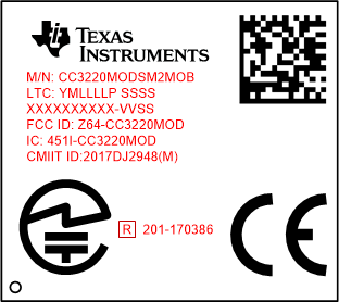
 

GUID-59126243-90D4-416C-937C-B6953F9660A6-low.gifFigure 9-2 CC3220MODS Module Marking
GUID-93A17C62-5BD0-45F9-997C-4021701E8BC7-low.gifFigure 9-3 CC3220MODSF Module Marking


Figure 9-4 and Figure 9-5 show the markings for the SimpleLink™ CC3220MODAx modules.
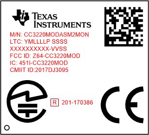
 

GUID-0B5AB2A5-80BE-439F-95D9-2DAA8963354F-low.gifFigure 9-4 CC3220MODAS Module Marking
GUID-13AC2C1F-D7D3-4001-AE7D-8616662DB760-low.gifFigure 9-5 CC3220MODASF Module Marking

Table 9-7 lists the CC3220MODx and CC3220MODAx module markings.

Table 9-7 Module Descriptions
MARKING DESCRIPTION
CC3220MODSM2MOB Model
CC3220MODSF12MOB
CC3220MODASM2MON
CC3220MODASF12MON
YMLLLLP SSSS LTC (lot trace code):
  • Y = Year
  • M = Month
  • LLLL = Assembly lot code
  • P = Reserved for internal use
  • SSSS = Serial number
XXXXXXXXXX-VVSS TI internal use only
Z64-CC3220MOD FCC ID: single modular FCC grant ID
451I-CC3220MOD IC: single modular IC grant ID
2017DJ2946(M) CMIIT: limited modular SRRC grant ID
2017DJ2944(M) CMIIT: limited modular SRRC grant ID
2017DJ3095 CMIIT: full modular SRRC grant ID
2017DJ3121 CMIIT: full modular SRRC grant ID
GUID-FD0CAC28-2496-4B5E-9719-820EA8039A91-low.gif MIC compliance mark
GUID-5C5A647E-B6B7-4D60-851E-9C265DAE3248-low.gif MIC ID: modular MIC grant ID
CE CE compliance mark


Drawings are representative. Content or placement may vary from what is illustrated.