ZHCSM59B November   2014  – September 2020 CC3100MOD

PRODUCTION DATA  

  1. 特性
  2. 应用
  3. 说明
  4. 功能方框图
  5. 功能方框图
  6. Revision History
  7. Terminal Configuration and Functions
    1. 7.1 CC3100MOD Pin Diagram
    2. 7.2 Pin Attributes
      1.      10
  8. Specifications
    1. 8.1  Absolute Maximum Ratings
    2. 8.2  ESD Ratings
    3. 8.3  Power-On Hours (POH)
    4. 8.4  Recommended Operating Conditions
    5. 8.5  Power Consumption Summary
    6. 8.6  TX Power and IBAT versus TX Power Level Settings
    7. 8.7  Brownout and Blackout Conditions
    8. 8.8  Electrical Characteristics (3.3 V, 25°C)
    9. 8.9  WLAN RF Characteristics
      1. 8.9.1 WLAN Receiver Characteristics
      2. 8.9.2 WLAN Transmitter Characteristics
    10. 8.10 Reset Requirement
    11. 8.11 Thermal Resistance Characteristics for MOB Package
    12. 8.12 Timing and Switching Characteristics
      1. 8.12.1 Wake-Up Sequence
      2. 8.12.2 Wake Up From Hibernate
        1. 8.12.2.1 nHIB Timing Requirements (1)
      3. 8.12.3 Interfaces
        1. 8.12.3.1 Host SPI Interface Timing
        2. 8.12.3.2 SPI Host Interface
    13. 8.13 Host UART
      1. 8.13.1 5-Wire UART Topology
      2. 8.13.2 4-Wire UART Topology
      3. 8.13.3 3-Wire UART Topology
  9. Detailed Description
    1. 9.1 Overview
    2. 9.2 Module Features
      1. 9.2.1 WLAN
      2. 9.2.2 Network Stack
      3. 9.2.3 Host Interface and Driver
      4. 9.2.4 System
    3. 9.3 Functional Block Diagram
    4. 9.4 Wi-Fi Network Processor Subsystem
    5. 9.5 Power-Management Subsystem
      1. 9.5.1 VBAT Wide-Voltage Connection
    6. 9.6 Low-Power Operating Modes
      1. 9.6.1 Low-Power Deep Sleep
      2. 9.6.2 Hibernate
  10. 10Applications, Implementation, and Layout
    1. 10.1 Reference Schematics
    2. 10.2 Design Requirements
    3. 10.3 Layout Recommendations
      1. 10.3.1 RF Section (Placement and Routing)
      2. 10.3.2 Antenna Placement and Routing
      3. 10.3.3 Transmission Line Considerations
  11. 11Environmental Requirements and Specifications
    1. 11.1 Temperature
      1. 11.1.1 PCB Bending
    2. 11.2 Handling Environment
      1. 11.2.1 Terminals
      2. 11.2.2 Falling
    3. 11.3 Storage Condition
      1. 11.3.1 Moisture Barrier Bag Before Opened
      2. 11.3.2 Moisture Barrier Bag Open
    4. 11.4 Baking Conditions
    5. 11.5 Soldering and Reflow Condition
  12. 12Device and Documentation Support
    1. 12.1 Device Support
      1. 12.1.1 Development Support
        1. 12.1.1.1 Firmware Updates
      2. 12.1.2 Device Nomenclature
    2. 12.2 Documentation Support
    3. 12.3 Trademarks
    4. 12.4 静电放电警告
    5. 12.5 术语表
  13. 13Mechanical, Packaging, and Orderable Information
    1. 13.1 Mechanical Drawing
    2. 13.2 Package Option
      1. 13.2.1 Packaging Information
      2. 13.2.2 Tape and Reel Information

封装选项

请参考 PDF 数据表获取器件具体的封装图。

机械数据 (封装 | 引脚)
  • MOB|63
散热焊盘机械数据 (封装 | 引脚)
订购信息

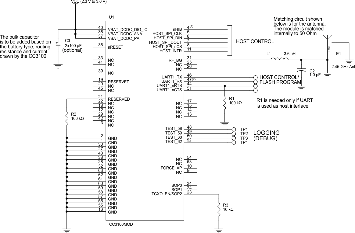
Reference Schematics

#SWRS1619015 shows the reference schematic for the CC3100MOD module. The complete schematic can be downloaded from http://www.ti.com/lit/zip/swrc293.
GUID-87042277-7619-4200-A705-0C6DD8A728DA-low.gif
If the GPIO from the MCU can float while the MCU enters low power, consider adding a pulldown resistor on the board to avoid floating.
TI recommends using a 100-kΩ pullup resistor to save a few tens of µA in hibernate state.
This is the reference schematic and not an actual board design. For the board files, refer to the CC3100MODBOOST in the CC3100MOD Tools Folder.
Figure 10-1 CC3100MOD Module Reference Schematic