ZHCSM59B November   2014  – September 2020 CC3100MOD

PRODUCTION DATA  

  1. 特性
  2. 应用
  3. 说明
  4. 功能方框图
  5. 功能方框图
  6. Revision History
  7. Terminal Configuration and Functions
    1. 7.1 CC3100MOD Pin Diagram
    2. 7.2 Pin Attributes
      1.      10
  8. Specifications
    1. 8.1  Absolute Maximum Ratings
    2. 8.2  ESD Ratings
    3. 8.3  Power-On Hours (POH)
    4. 8.4  Recommended Operating Conditions
    5. 8.5  Power Consumption Summary
    6. 8.6  TX Power and IBAT versus TX Power Level Settings
    7. 8.7  Brownout and Blackout Conditions
    8. 8.8  Electrical Characteristics (3.3 V, 25°C)
    9. 8.9  WLAN RF Characteristics
      1. 8.9.1 WLAN Receiver Characteristics
      2. 8.9.2 WLAN Transmitter Characteristics
    10. 8.10 Reset Requirement
    11. 8.11 Thermal Resistance Characteristics for MOB Package
    12. 8.12 Timing and Switching Characteristics
      1. 8.12.1 Wake-Up Sequence
      2. 8.12.2 Wake Up From Hibernate
        1. 8.12.2.1 nHIB Timing Requirements (1)
      3. 8.12.3 Interfaces
        1. 8.12.3.1 Host SPI Interface Timing
        2. 8.12.3.2 SPI Host Interface
    13. 8.13 Host UART
      1. 8.13.1 5-Wire UART Topology
      2. 8.13.2 4-Wire UART Topology
      3. 8.13.3 3-Wire UART Topology
  9. Detailed Description
    1. 9.1 Overview
    2. 9.2 Module Features
      1. 9.2.1 WLAN
      2. 9.2.2 Network Stack
      3. 9.2.3 Host Interface and Driver
      4. 9.2.4 System
    3. 9.3 Functional Block Diagram
    4. 9.4 Wi-Fi Network Processor Subsystem
    5. 9.5 Power-Management Subsystem
      1. 9.5.1 VBAT Wide-Voltage Connection
    6. 9.6 Low-Power Operating Modes
      1. 9.6.1 Low-Power Deep Sleep
      2. 9.6.2 Hibernate
  10. 10Applications, Implementation, and Layout
    1. 10.1 Reference Schematics
    2. 10.2 Design Requirements
    3. 10.3 Layout Recommendations
      1. 10.3.1 RF Section (Placement and Routing)
      2. 10.3.2 Antenna Placement and Routing
      3. 10.3.3 Transmission Line Considerations
  11. 11Environmental Requirements and Specifications
    1. 11.1 Temperature
      1. 11.1.1 PCB Bending
    2. 11.2 Handling Environment
      1. 11.2.1 Terminals
      2. 11.2.2 Falling
    3. 11.3 Storage Condition
      1. 11.3.1 Moisture Barrier Bag Before Opened
      2. 11.3.2 Moisture Barrier Bag Open
    4. 11.4 Baking Conditions
    5. 11.5 Soldering and Reflow Condition
  12. 12Device and Documentation Support
    1. 12.1 Device Support
      1. 12.1.1 Development Support
        1. 12.1.1.1 Firmware Updates
      2. 12.1.2 Device Nomenclature
    2. 12.2 Documentation Support
    3. 12.3 Trademarks
    4. 12.4 静电放电警告
    5. 12.5 术语表
  13. 13Mechanical, Packaging, and Orderable Information
    1. 13.1 Mechanical Drawing
    2. 13.2 Package Option
      1. 13.2.1 Packaging Information
      2. 13.2.2 Tape and Reel Information

封装选项

请参考 PDF 数据表获取器件具体的封装图。

机械数据 (封装 | 引脚)
  • MOB|63
散热焊盘机械数据 (封装 | 引脚)
订购信息

Wake Up From Hibernate

#SWAS0318564 shows the timing diagram for wake up from the hibernate state.
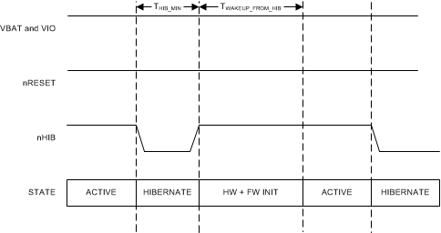
GUID-A15BF857-8564-46A4-A7F5-6F4A10C01915-low.gifFigure 8-7 nHIB Timing Diagram
Note:

The internal 32.768-kHz crystal oscillator is kept enabled by default when the chip goes to hibernate in response to nHIB being pulled low.

GUID-400CF46C-B651-457D-A1D7-C5F78DD51018.html#GUID-400CF46C-B651-457D-A1D7-C5F78DD51018 describes the timing requirements for nHIB.