ZHCSDC8A December   2014  – November 2017

PRODUCTION DATA.  

  1. 特性
  2. 应用
  3. 说明
    1.     bq24193 的 PSEL、USB On-The-Go (OTG) 和支持 JEITA 配置文件
  4. 修订历史记录
  5. 说明 (续)
  6. Pin Configuration and Functions
    1.     Pin Functions
  7. Specifications
    1. 7.1 Absolute Maximum Ratings
    2. 7.2 ESD Ratings
    3. 7.3 Recommended Operating Conditions
    4. 7.4 Thermal Information
    5. 7.5 Electrical Characteristics
    6. 7.6 Typical Characteristics
  8. Detailed Description
    1. 8.1 Overview
    2. 8.2 Functional Block Diagram
    3. 8.3 Feature Description
      1. 8.3.1 Device Power Up
        1. 8.3.1.1 Power-On-Reset (POR)
        2. 8.3.1.2 Power Up from Battery without DC Source
          1. 8.3.1.2.1 BATFET Turn Off
          2. 8.3.1.2.2 Shipping Mode
        3. 8.3.1.3 Power Up from DC Source
          1. 8.3.1.3.1 REGN LDO
          2. 8.3.1.3.2 Input Source Qualification
          3. 8.3.1.3.3 Input Current Limit Detection
          4. 8.3.1.3.4 PSEL/OTG Pins Set Input Current Limit
          5. 8.3.1.3.5 HIZ State wth 100mA USB Host
          6. 8.3.1.3.6 Force Input Current Limit Detection
        4. 8.3.1.4 Converter Power-Up
        5. 8.3.1.5 Boost Mode Operation from Battery
      2. 8.3.2 Power Path Management
        1. 8.3.2.1 Narrow VDC Architecture
        2. 8.3.2.2 Dynamic Power Management
        3. 8.3.2.3 Supplement Mode
      3. 8.3.3 Battery Charging Management
        1. 8.3.3.1 Autonomous Charging Cycle
        2. 8.3.3.2 Battery Charging Profile
        3. 8.3.3.3 Battery Path Impedance IR Compensation
        4. 8.3.3.4 Thermistor Qualification
          1. 8.3.3.4.1 JEITA Guideline Compliance
        5. 8.3.3.5 Charging Termination
          1. 8.3.3.5.1 Termination when REG02[0] = 1
          2. 8.3.3.5.2 Termination when REG05[6] = 1
        6. 8.3.3.6 Charging Safety Timer
        7. 8.3.3.7 USB Timer when Charging from USB100mA Source
      4. 8.3.4 Status Outputs (PG, STAT, and INT)
        1. 8.3.4.1 Power Good Indicator (PG)
        2. 8.3.4.2 Charging Status Indicator (STAT)
        3. 8.3.4.3 Interrupt to Host (INT)
      5. 8.3.5 Protections
        1. 8.3.5.1 Input Current Limit on ILIM
        2. 8.3.5.2 Thermal Regulation and Thermal Shutdown
        3. 8.3.5.3 Voltage and Current Monitoring in Buck Mode
          1. 8.3.5.3.1 Input Over-Voltage (ACOV)
          2. 8.3.5.3.2 System Over-Voltage Protection (SYSOVP)
        4. 8.3.5.4 Voltage and Current Monitoring in Boost Mode
          1. 8.3.5.4.1 VBUS Over-Voltage Protection
        5. 8.3.5.5 Battery Protection
          1. 8.3.5.5.1 Battery Over-Current Protection (BATOVP)
          2. 8.3.5.5.2 Charging During Battery Short Protection
          3. 8.3.5.5.3 System Over-Current Protection
      6. 8.3.6 Serial Interface
        1. 8.3.6.1 Data Validity
        2. 8.3.6.2 START and STOP Conditions
        3. 8.3.6.3 Byte Format
        4. 8.3.6.4 Acknowledge (ACK) and Not Acknowledge (NACK)
        5. 8.3.6.5 Slave Address and Data Direction Bit
          1. 8.3.6.5.1 Single Read and Write
          2. 8.3.6.5.2 Multi-Read and Multi-Write
    4. 8.4 Device Functional Modes
      1. 8.4.1 Host Mode and Default Mode
        1. 8.4.1.1 Plug in USB100mA Source with Good Battery
        2. 8.4.1.2 USB Timer when Charging from USB 100-mA Source
    5. 8.5 Register Map
      1. 8.5.1 I2C Registers
        1. 8.5.1.1  Input Source Control Register REG00 (reset = 00110000, or 30)
          1. Table 7. REG00 Input Source Control Register Description
        2. 8.5.1.2  Power-On Configuration Register REG01 (reset = 00011011, or 1B)
          1. Table 8. REG01 Power-On Configuration Register Description
        3. 8.5.1.3  Charge Current Control Register REG02 (reset = 01100000, or 60)
          1. Table 9. REG02 Charge Current Control Register Description
        4. 8.5.1.4  Pre-Charge/Termination Current Control Register REG03 (reset = 00010001, or 11)
          1. Table 10. REG03 Pre-Charge/Termination Current Control Register Description
        5. 8.5.1.5  Charge Voltage Control Register REG04 (reset = 10110010, or B2)
          1. Table 11. REG04 Charge Voltage Control Register Description
        6. 8.5.1.6  Charge Termination/Timer Control Register REG05 (reset = 10011010, or 9A)
          1. Table 12. REG05 Charge Termination/Timer Control Register Description
        7. 8.5.1.7  IR Compensation / Thermal Regulation Control Register REG06 (reset = 00000011, or 03)
          1. Table 13. REG06 IR Compensation / Thermal Regulation Control Register Description
        8. 8.5.1.8  Misc Operation Control Register REG07 (reset = 01001011, or 4B)
          1. Table 14. REG07 Misc Operation Control Register Description
        9. 8.5.1.9  System Status Register REG08
          1. Table 15. REG08 System Status Register Description
        10. 8.5.1.10 Fault Register REG09
          1. Table 16. REG09 Fault Register Description
        11. 8.5.1.11 Vender / Part / Revision Status Register REG0A (reset = 00101111, or 2F)
          1. Table 17. REG0A Vender / Part / Revision Status Register Description
  9. Application and Implementation
    1. 9.1 Application Information
    2. 9.2 Typical Application
      1. 9.2.1 Design Requirements
      2. 9.2.2 Detailed Design Procedure
        1. 9.2.2.1 Inductor Selection
        2. 9.2.2.2 Input Capacitor
        3. 9.2.2.3 Output Capacitor
      3. 9.2.3 Application Performance Plots
  10. 10Power Supply Recommendations
  11. 11Layout
    1. 11.1 Layout Guidelines
    2. 11.2 Layout Example
  12. 12器件和文档支持
    1. 12.1 文档支持
      1. 12.1.1 相关文档
    2. 12.2 接收文档更新通知
    3. 12.3 社区资源
    4. 12.4 商标
    5. 12.5 静电放电警告
    6. 12.6 Glossary
  13. 13机械、封装和可订购信息

封装选项

机械数据 (封装 | 引脚)
散热焊盘机械数据 (封装 | 引脚)
订购信息

JEITA Guideline Compliance

To improve the safety of charging Li-ion batteries, JEITA guideline was released on April 20, 2007. The guideline emphasized the importance of avoiding a high charge current and high charge voltage at certain low and high temperature ranges.

To initiate a charge cycle, the voltage on TS pin must be within the VT1 to VT5 thresholds. If TS voltage exceeds the T1–T5 range, the controller suspends charging and waits until the battery temperature is within the T1 to T5 range. At cool temperature (T1–T2), JEITA recommends the charge current to be reduced to at least half of the charge current or lower. At warm temperature (T3–T5), JEITA recommends charge voltage less than 4.1 V.

The bq24193 provides flexibility voltage/current settings beyond the JEITA requirement. The voltage setting at warm temperature (T3–T5) can be 4.2 V or 4.05 V (REG07 bit[4]). The current setting at cool temperature (T1–T2) can be further reduced to 20% of fast charge current (REG05 bit[0]).
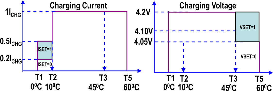
bq24193 JEITA_Charging_Profile_SLUSBG8.gif

The resistor bias network has been updated as below.
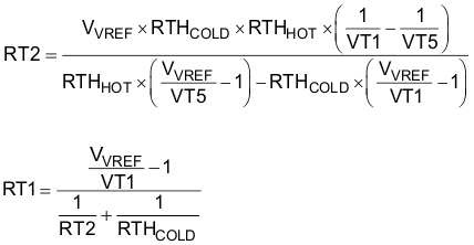
Equation 2. bq24193 Eq2_slusaw5.gif

Select 0°C to 60°C range for Li-ion or Li-polymer battery,
RTHT1 = 27.28 kΩ
RTHT5 = 3.02 kΩ
RT1 = 2.27 kΩ
RT2 = 6.86 kΩ