ZHCSPA6F September 2006 – January 2022
PRODUCTION DATA
- 1 特性
- 2 应用
- 3 说明
- 4 Revision History
- 5 Pin Configuration and Functions
- 6 Specifications
-
7 Detailed Description
- 7.1 Overview
- 7.2 Functional Block Diagram
- 7.3 Feature Description
- 7.4 Device Functional Modes
- 7.5
Programming
- 7.5.1 Serial Communication
- 7.5.2 Initialization
- 7.5.3 ROM Commands
- 7.5.4 Memory/Status Function Commands
- 7.5.5 READ MEMORY Commands
- 7.5.6 WRITE MEMORY Command
- 7.5.7 READ STATUS Command
- 7.5.8 WRITE STATUS Command
- 7.5.9 PROGRAM PROFILE Byte
- 7.5.10 SDQ Signaling
- 7.5.11 RESET and PRESENCE PULSE
- 7.5.12 WRITE Bit
- 7.5.13 READ Bit
- 7.5.14 PROGRAM PULSE
- 7.5.15 IDLE
- 7.5.16 CRC Generation
- 8 Application and Implementation
- 9 Power Supply Recommendations
- 10Layout
- 11Device and Documentation Support
- 12Mechanical, Packaging, and Orderable Information
8.2.2.1 Programming Circuit Example
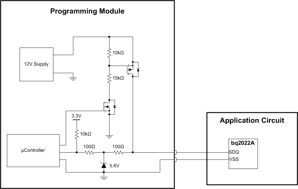
The BQ2022A requires a 12-V maximum pulse signal to program the OTP memory. It is necessary to have a programming test setup for production. Figure 8-2 shows an example of what the circuit could be for such setup. The Programming Module contains the microcontroller that acts as SDQ master and also controls the time of the programming pulse and its width. The 12-V supply is the source for the programming pulse. Only SDQ and VSS signals need to exit the test setup as the Application Circuit containing the BQ2022A under test is connected only for programming and verifying data.
The Programming Module typically will connect to a PC using interface such as USB. The diagram in Figure 8-2 does not include the interface to a PC which can vary depending on the system designer's choice.
 Figure 8-2 BQ2022A
Programming Circuit Example