ZHCSPA6F September 2006 – January 2022
PRODUCTION DATA
- 1 特性
- 2 应用
- 3 说明
- 4 Revision History
- 5 Pin Configuration and Functions
- 6 Specifications
-
7 Detailed Description
- 7.1 Overview
- 7.2 Functional Block Diagram
- 7.3 Feature Description
- 7.4 Device Functional Modes
- 7.5
Programming
- 7.5.1 Serial Communication
- 7.5.2 Initialization
- 7.5.3 ROM Commands
- 7.5.4 Memory/Status Function Commands
- 7.5.5 READ MEMORY Commands
- 7.5.6 WRITE MEMORY Command
- 7.5.7 READ STATUS Command
- 7.5.8 WRITE STATUS Command
- 7.5.9 PROGRAM PROFILE Byte
- 7.5.10 SDQ Signaling
- 7.5.11 RESET and PRESENCE PULSE
- 7.5.12 WRITE Bit
- 7.5.13 READ Bit
- 7.5.14 PROGRAM PULSE
- 7.5.15 IDLE
- 7.5.16 CRC Generation
- 8 Application and Implementation
- 9 Power Supply Recommendations
- 10Layout
- 11Device and Documentation Support
- 12Mechanical, Packaging, and Orderable Information
7.5.6 WRITE MEMORY Command
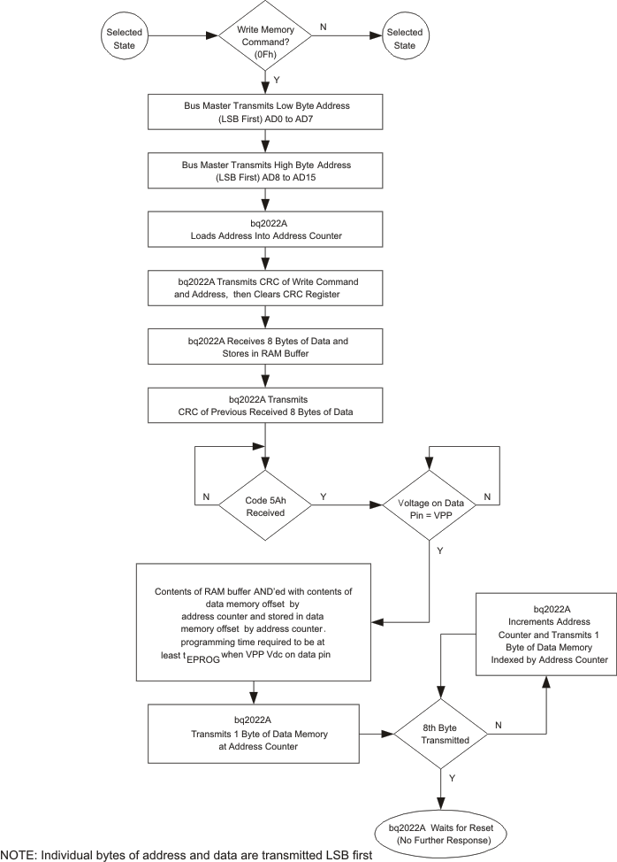
The WRITE MEMORY command is used to program the 1024-bit EPROM memory field. The 1024-bit memory field is programmed in 8-byte segments. Data is first written into an 8-byte RAM buffer one byte at a time. The contents of the RAM buffer is then ANDed with the contents of the EPROM memory field when the programming command is issued.
Figure 7-5 illustrates the sequence of events for programming the EPROM memory field. After issuing a SKIP ROM command, the host issues the WRITE MEMORY command, 0Fh, followed by the low byte and then the high byte of the starting address. The BQ2022A calculates and transmits an 8-bit CRC based on the WRITE command and address.
If at any time during the WRITE MEMORY process, the CRC read by the host is incorrect, a reset pulse must be issued, and the entire sequence must be repeated.
After the BQ2022A transmits the CRC, the host then transmits 8 bytes of data to the BQ2022A. Another 8-bit CRC is calculated and transmitted based on the 8 bytes of data. If this CRC agrees with the CRC calculated by the host, the host transmits the program command 5Ah and then applies the programming voltage for at least 2500 μs or tEPROG. The contents of the RAM buffer is then logically ANDed with the contents of the 8-byte EPROM offset by the starting address.
The starting address can be any integer multiple of eight between 0000 and 007F (hex) such as 0000, 0008, and 0010 (hex).
The WRITE DATA MEMORY command sequence can be terminated at any point by issuing a reset pulse except during the program pulse period tPROG.
The BQ2022A responds with the data from the selected EPROM address sent least significant-bit first. This response should be checked to verify the programmed byte. If the programmed byte is incorrect, then the host must reset the part and begin the write sequence again.
For both of these cases, the decision to continue programming is made entirely by the host, because the BQ2022A is not able to determine if the 8-bit CRC calculated by the host agrees with the 8-bit CRC calculated by the BQ2022A.
Prior to programming, bits in the 1024-bit EPROM data field appear as logical 1 s.
 Figure 7-5 WRITE MEMORY Command Flow