ZHCSHT7E April   2019  – February 2023 ADC12DJ5200RF

PRODUCTION DATA  

  1. 特性
  2. 应用
  3. 说明
  4. Revision History
  5. Pin Configuration and Functions
  6. Specifications
    1. 6.1  Absolute Maximum Ratings
    2. 6.2  ESD Ratings
    3. 6.3  Recommended Operating Conditions
    4. 6.4  Thermal Information
    5. 6.5  Electrical Characteristics: DC Specifications
    6. 6.6  Electrical Characteristics: Power Consumption
    7. 6.7  Electrical Characteristics: AC Specifications (Dual-Channel Mode)
    8. 6.8  Electrical Characteristics: AC Specifications (Single-Channel Mode)
    9. 6.9  Timing Requirements
    10. 6.10 Switching Characteristics
    11. 6.11 Typical Characteristics
  7. Detailed Description
    1. 7.1 Overview
    2. 7.2 Functional Block Diagram
    3. 7.3 Feature Description
      1. 7.3.1  Device Comparison
      2. 7.3.2  Analog Inputs
        1. 7.3.2.1 Analog Input Protection
        2. 7.3.2.2 Full-Scale Voltage (VFS) Adjustment
        3. 7.3.2.3 Analog Input Offset Adjust
      3. 7.3.3  ADC Core
        1. 7.3.3.1 ADC Theory of Operation
        2. 7.3.3.2 ADC Core Calibration
        3. 7.3.3.3 Analog Reference Voltage
        4. 7.3.3.4 ADC Overrange Detection
        5. 7.3.3.5 Code Error Rate (CER)
      4. 7.3.4  Temperature Monitoring Diode
      5. 7.3.5  Timestamp
      6. 7.3.6  Clocking
        1. 7.3.6.1 Noiseless Aperture Delay Adjustment (tAD Adjust)
        2. 7.3.6.2 Aperture Delay Ramp Control (TAD_RAMP)
        3. 7.3.6.3 SYSREF Capture for Multi-Device Synchronization and Deterministic Latency
          1. 7.3.6.3.1 SYSREF Position Detector and Sampling Position Selection (SYSREF Windowing)
          2. 7.3.6.3.2 Automatic SYSREF Calibration
      7. 7.3.7  Programmable FIR Filter (PFIR)
        1. 7.3.7.1 Dual Channel Equalization
        2. 7.3.7.2 Single Channel Equalization
        3. 7.3.7.3 Time Varying Filter
      8. 7.3.8  Digital Down Converters (DDC)
        1. 7.3.8.1 Rounding and Saturation
        2. 7.3.8.2 Numerically-Controlled Oscillator and Complex Mixer
          1. 7.3.8.2.1 NCO Fast Frequency Hopping (FFH)
          2. 7.3.8.2.2 NCO Selection
          3. 7.3.8.2.3 Basic NCO Frequency Setting Mode
          4. 7.3.8.2.4 Rational NCO Frequency Setting Mode
          5. 7.3.8.2.5 NCO Phase Offset Setting
          6. 7.3.8.2.6 NCO Phase Synchronization
        3. 7.3.8.3 Decimation Filters
        4. 7.3.8.4 Output Data Format
        5. 7.3.8.5 Decimation Settings
          1. 7.3.8.5.1 Decimation Factor
          2. 7.3.8.5.2 DDC Gain Boost
      9. 7.3.9  JESD204C Interface
        1. 7.3.9.1 Transport Layer
        2. 7.3.9.2 Scrambler
        3. 7.3.9.3 Link Layer
        4. 7.3.9.4 8B/10B Link Layer
          1. 7.3.9.4.1 Data Encoding (8B/10B)
          2. 7.3.9.4.2 Multiframes and the Local Multiframe Clock (LMFC)
          3. 7.3.9.4.3 Code Group Synchronization (CGS)
          4. 7.3.9.4.4 Initial Lane Alignment Sequence (ILAS)
          5. 7.3.9.4.5 Frame and Multiframe Monitoring
        5. 7.3.9.5 64B/66B Link Layer
          1. 7.3.9.5.1 64B/66B Encoding
          2. 7.3.9.5.2 Multiblocks, Extended Multiblocks and the Local Extended Multiblock Clock (LEMC)
          3. 7.3.9.5.3 Block, Multiblock and Extended Multiblock Alignment using Sync Header
            1. 7.3.9.5.3.1 Cyclic Redundancy Check (CRC) Mode
            2. 7.3.9.5.3.2 Forward Error Correction (FEC) Mode
          4. 7.3.9.5.4 Initial Lane Alignment
          5. 7.3.9.5.5 Block, Multiblock and Extended Multiblock Alignment Monitoring
        6. 7.3.9.6 Physical Layer
          1. 7.3.9.6.1 SerDes Pre-Emphasis
        7. 7.3.9.7 JESD204C Enable
        8. 7.3.9.8 Multi-Device Synchronization and Deterministic Latency
        9. 7.3.9.9 Operation in Subclass 0 Systems
      10. 7.3.10 Alarm Monitoring
        1. 7.3.10.1 Clock Upset Detection
        2. 7.3.10.2 FIFO Upset Detection
    4. 7.4 Device Functional Modes
      1. 7.4.1 Dual-Channel Mode
      2. 7.4.2 Single-Channel Mode (DES Mode)
      3. 7.4.3 Dual-Input Single-Channel Mode (DUAL DES Mode)
      4. 7.4.4 JESD204C Modes
        1. 7.4.4.1 JESD204C Operating Modes Table
        2. 7.4.4.2 JESD204C Modes continued
        3. 7.4.4.3 JESD204C Transport Layer Data Formats
        4. 7.4.4.4 64B/66B Sync Header Stream Configuration
        5. 7.4.4.5 Dual DDC and Redundant Data Mode
      5. 7.4.5 Power-Down Modes
      6. 7.4.6 Test Modes
        1. 7.4.6.1 Serializer Test-Mode Details
        2. 7.4.6.2 PRBS Test Modes
        3. 7.4.6.3 Clock Pattern Mode
        4. 7.4.6.4 Ramp Test Mode
        5. 7.4.6.5 Short and Long Transport Test Mode
          1. 7.4.6.5.1 Short Transport Test Pattern
        6. 7.4.6.6 D21.5 Test Mode
        7. 7.4.6.7 K28.5 Test Mode
        8. 7.4.6.8 Repeated ILA Test Mode
        9. 7.4.6.9 Modified RPAT Test Mode
      7. 7.4.7 Calibration Modes and Trimming
        1. 7.4.7.1 Foreground Calibration Mode
        2. 7.4.7.2 Background Calibration Mode
        3. 7.4.7.3 Low-Power Background Calibration (LPBG) Mode
      8. 7.4.8 Offset Calibration
      9. 7.4.9 Trimming
    5. 7.5 Programming
      1. 7.5.1 Using the Serial Interface
        1. 7.5.1.1 SCS
        2. 7.5.1.2 SCLK
        3. 7.5.1.3 SDI
        4. 7.5.1.4 SDO
        5. 7.5.1.5 Streaming Mode
    6. 7.6 SPI Register Map
  8. Application Information Disclaimer
    1. 8.1 Application Information
    2. 8.2 Typical Applications
      1. 8.2.1 Wideband RF Sampling Receiver
        1. 8.2.1.1 Design Requirements
          1. 8.2.1.1.1 Input Signal Path
          2. 8.2.1.1.2 Clocking
        2. 8.2.1.2 Detailed Design Procedure
          1. 8.2.1.2.1 Calculating Values of AC-Coupling Capacitors
        3. 8.2.1.3 Application Curves
      2. 8.2.2 Reconfigurable Dual-Channel 5-GSPS or Single-Channel 10-Gsps Oscilloscope
        1. 8.2.2.1 Design Requirements
          1. 8.2.2.1.1 Input Signal Path
          2. 8.2.2.1.2 Clocking
          3. 8.2.2.1.3 ADC12DJ5200RF
        2. 8.2.2.2 Application Curves
    3. 8.3 Initialization Set Up
  9. Power Supply Recommendations
    1. 9.1 Power Sequencing
  10. 10Layout
    1. 10.1 Layout Guidelines
    2. 10.2 Layout Example
  11. 11Device and Documentation Support
    1. 11.1 Device Support
      1. 11.1.1 Development Support
        1. 11.1.1.1 146
    2. 11.2 Documentation Support
      1. 11.2.1 Related Documentation
    3. 11.3 Receiving Notification of Documentation Updates
    4. 11.4 Support Resources
    5. 11.5 Trademarks
    6. 11.6 静电放电警告
    7. 11.7 术语表
  12. 12Mechanical, Packaging, and Orderable Information

封装选项

机械数据 (封装 | 引脚)
散热焊盘机械数据 (封装 | 引脚)
订购信息
Rational NCO Frequency Setting Mode

In basic NCO frequency mode, the frequency step size is very small and many frequencies can be synthesized, but sometimes an application requires very specific frequencies that fall between two frequency steps. For example with ƒS equal to 2457.6 MHz and a desired ƒ(NCO) equal to 5.02 MHz, the value for FREQAx is 8773085.867. Truncating the fractional portion results in an ƒ(NCO) equal to 5.0199995 MHz, which is not the desired frequency.

To produce the desired frequency, the NCO_RDIV parameter is used to force the phase accumulator to arrive at specific frequencies without error. First, select a frequency step size (ƒ(STEP)) that is appropriate for the NCO frequency steps required. The typical value of ƒ(STEP) is 10 kHz. Next, use Equation 6 to program the NCO_RDIV value.

Equation 6. GUID-95DFBAB2-0413-438E-940D-CEA6AAD86CCD-low.gif

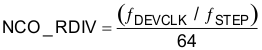
The result of Equation 6 must be an integer value. If the value is not an integer, adjust either of the parameters until the result is an integer value.

For example, select a value of 1920 for NCO_RDIV.

Note:

NCO_RDIV values larger than 8192 can degrade the NCO SFDR performance and are not recommended.

Now use Equation 7 to calculate the FREQAx register value.

Equation 7. GUID-7DEA0A9B-7F1B-424D-9A26-0A57ECF9D456-low.gif

Alternatively, the following equations can be used:

Equation 8. GUID-9AC99143-9EDD-412B-9E02-8BCCE7E4256B-low.gif
Equation 9. GUID-58FE9CB6-FFC8-4D42-B9A8-38D9977B699F-low.gif

#GUID-50B57ED5-A1F3-4EED-85B5-491B2EE2DAA8/SLVSEN9239 lists common values for NCO_RDIV in 10-kHz frequency steps.

Table 7-11 Common NCO_RDIV Values (For 10-kHz Frequency Steps)
fCLK (MHz)NCO_RDIV
2457.63840
1966.083072
16002500
1474.562304
1228.81920