ZHCSEC5D November 2015 – May 2021 TPS65235
PRODUCTION DATA
- 1 特性
- 2 应用
- 3 说明
- 4 Revision History
- 5 Pin Configuration and Functions
- 6 Specifications
-
7 Detailed Description
- 7.1 Overview
- 7.2 Functional Block Diagram
- 7.3
Feature Description
- 7.3.1 Boost Converter
- 7.3.2 Linear Regulator and Current Limit
- 7.3.3 Boost Converter Current Limit
- 7.3.4 Charge Pump
- 7.3.5 Slew Rate Control
- 7.3.6 Short Circuit Protection, Hiccup and Overtemperature Protection
- 7.3.7 Tone Generation
- 7.3.8 Tone Detection
- 7.3.9 Disable and Enable
- 7.3.10 Component Selection
- 7.4 Device Functional Modes
- 7.5 Programming
- 7.6 Register Maps
- 8 Application and Implementation
- 9 Power Supply Recommendations
- 10Layout
- 11Device and Documentation Support
- 12Mechanical, Packaging, and Orderable Information
7.3.5 Slew Rate Control
When LNB output voltage transits from 13.4 V to 18.2 V or 18.2 V to 13.4 V, the cap at pin TCAP controls the transition time. This transition time makes sure the boost converter output to follow LNB output change. Usually boost converter has low bandwidth and can’t response fast. The voltage at TCAP acts as the reference voltage of the linear regulator. The boost converter’s reference is also based on TCAP with additional fixed voltage to generate a 0.8 V above the LNB output.
The charging and discharging current is 10 µA, thus the transition time can be estimated as:
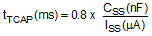
A 22-nF capacitor generates about 2 ms transition time.
In light load conditions, when LNB output voltage is set from 18.2 V to 13.4 V, the voltage drops very slow, which causes wrong VOUT_GOOD (Bit 0 at status register 0x02) logic for LNB output voltage detection. TPS65235 has integrated a pull down circuit to pull down the output during the transition. This ensures the voltage change can follow the voltage at TCAP. When the 22-kHz tone signal is superimposing on the LNB output voltage, the pull down current can also provide square wave instead of a distorted waveforms.