ZHCSEC5D November 2015 – May 2021 TPS65235
PRODUCTION DATA
- 1 特性
- 2 应用
- 3 说明
- 4 Revision History
- 5 Pin Configuration and Functions
- 6 Specifications
-
7 Detailed Description
- 7.1 Overview
- 7.2 Functional Block Diagram
- 7.3
Feature Description
- 7.3.1 Boost Converter
- 7.3.2 Linear Regulator and Current Limit
- 7.3.3 Boost Converter Current Limit
- 7.3.4 Charge Pump
- 7.3.5 Slew Rate Control
- 7.3.6 Short Circuit Protection, Hiccup and Overtemperature Protection
- 7.3.7 Tone Generation
- 7.3.8 Tone Detection
- 7.3.9 Disable and Enable
- 7.3.10 Component Selection
- 7.4 Device Functional Modes
- 7.5 Programming
- 7.6 Register Maps
- 8 Application and Implementation
- 9 Power Supply Recommendations
- 10Layout
- 11Device and Documentation Support
- 12Mechanical, Packaging, and Orderable Information
7.3.10.2 Capacitor Selection
TPS65235 has a 1 MHz non‐synchronous boost converter integrated and the boost converter features the internal compensation network. TPS65235 works well with both ceramic capacitor and electrolytic capacitor.
In TPS65235 application, the recommended ceramic capacitors rated are at least X7R/X5R, 35 V rating and 1206 size for the achieving lower LNB output ripple. Table 7-1 shows the recommended ceramic capacitors list for both 4.7uH and 10uH boost inductors.
If lower cost is demanded, a 100-µF electrolytic (Low ESR) and a 10-µF/35-V ceramic capacitor also work well, this solution provides lower system cost.
| Boost Inductor | Capacitors | Tolerance (%) | Rating (V) | Size |
|---|---|---|---|---|
| 10 µH | 2 x 22 µF | ±10 | 35 | 1206 |
| 2 x 10 µF | ±10 | 35 | 1206 | |
| 4.7 µH | 2 x 22 µF | ±10 | 35 | 1206 |
| 2 x 10 µF | ±10 | 35 | 1206 | |
| 22 µF | ±10 | 35 | 1206 |
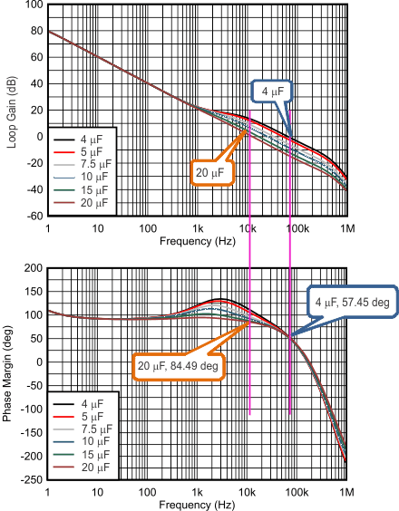
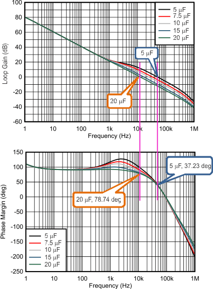
Figure 7-6 and Figure 7-7 show a Bode plot of boost loop with 4.7 µH / 10 µH inductance and 4 µF, 5 µF, 7.5 µF, 10 µF, 15 µF and 20 µF of boost capacitance after degrading. As the boost capacitance increases, the phase margin decreases.
 Figure 7-6 Gain and Phase Margin of the Boost Loop With Different Boost Capacitance (VIN = 12 V, VOUT = 18.2 V, ILOAD = 1 A, FSW = 1 MHz, 4.7 µH, Typical Bode Plot)
 Figure 7-7 Gain and Phase Margin of the Boost Loop With Different Boost Capacitance (VIN = 12 V, VOUT = 18.2 V, ILOAD = 1 A, FSW = 1 MHz, 10 µH, Typical Bode Plot)