ZHCS181G August 2011 – April 2021 TPS53355
PRODUCTION DATA
- 1 特性
- 2 应用
- 3 说明
- 4 Revision History
- 5 Pin Configuration and Functions
- 6 Specifications
-
7 Detailed Description
- 7.1 Overview
- 7.2 Functional Block Diagram
- 7.3
Feature Description
- 7.3.1 5-V LDO and VREG Start-Up
- 7.3.2 Adaptive On-Time D-CAP Control and Frequency Selection
- 7.3.3 Ramp Signal
- 7.3.4 Adaptive Zero Crossing
- 7.3.5 Power-Good
- 7.3.6 Current Sense, Overcurrent and Short Circuit Protection
- 7.3.7 Overvoltage and Undervoltage Protection
- 7.3.8 UVLO Protection
- 7.3.9 Thermal Shutdown
- 7.4 Device Functional Modes
- 8 Application and Implementation
- 9 Power Supply Recommendations
- 10Layout
- 11Device and Documentation Support
- 12Mechanical, Packaging, and Orderable Information
封装选项
请参考 PDF 数据表获取器件具体的封装图。
机械数据 (封装 | 引脚)
- DQP|22
散热焊盘机械数据 (封装 | 引脚)
- DQP|22
订购信息
8.1.1 Small Signal Model
From small-signal loop analysis, a buck converter using D-CAP™ mode can be simplified as shown in Figure 8-1.
 Figure 8-1 Simplified Modulator Model
The output voltage is compared with the internal reference voltage (ramp signal is ignored here for simplicity). The PWM comparator determines the timing to turn on the high-side MOSFET. The gain and speed of the comparator can be assumed high enough to keep the voltage at the beginning of each on cycle substantially constant.
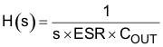
For loop stability, the 0-dB frequency, ƒ0, defined below need to be lower than 1/4 of the switching frequency.
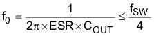
According to the equation above, the loop stability of D-CAPTM mode modulator is mainly determined by the capacitor's chemistry. For example, specialty polymer capacitors (SP-CAP) have an output capacitance in the order of several 100 µF and ESR in range of 10 mΩ. These makes ƒ0 on the order of 100 kHz or less, creating a stable loop. However, ceramic capacitors have an ƒ0 at more than 700 kHz, and need special care when used with this modulator. An application circuit for ceramic capacitor is described in Section 8.2.1.2.3.