ZHCS181G August 2011 – April 2021 TPS53355
PRODUCTION DATA
- 1 特性
- 2 应用
- 3 说明
- 4 Revision History
- 5 Pin Configuration and Functions
- 6 Specifications
-
7 Detailed Description
- 7.1 Overview
- 7.2 Functional Block Diagram
- 7.3
Feature Description
- 7.3.1 5-V LDO and VREG Start-Up
- 7.3.2 Adaptive On-Time D-CAP Control and Frequency Selection
- 7.3.3 Ramp Signal
- 7.3.4 Adaptive Zero Crossing
- 7.3.5 Power-Good
- 7.3.6 Current Sense, Overcurrent and Short Circuit Protection
- 7.3.7 Overvoltage and Undervoltage Protection
- 7.3.8 UVLO Protection
- 7.3.9 Thermal Shutdown
- 7.4 Device Functional Modes
- 8 Application and Implementation
- 9 Power Supply Recommendations
- 10Layout
- 11Device and Documentation Support
- 12Mechanical, Packaging, and Orderable Information
封装选项
请参考 PDF 数据表获取器件具体的封装图。
机械数据 (封装 | 引脚)
- DQP|22
散热焊盘机械数据 (封装 | 引脚)
- DQP|22
订购信息
6.6 Typical Characteristics
For VOUT = 5 V, a 744355182 inductor is used. For 1 ≤ VOUT ≤ 3.3 V, a PA0513.441 inductor is used.
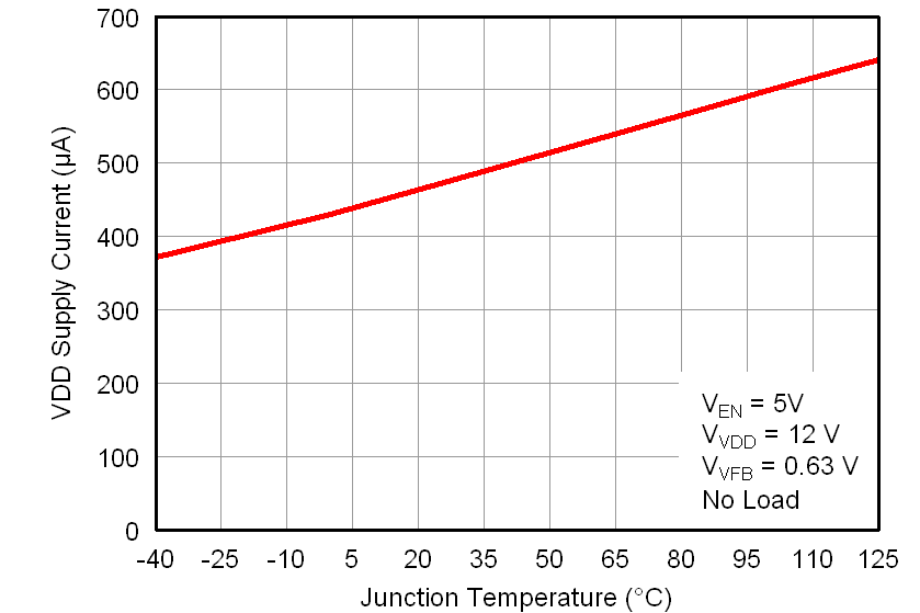 Figure 6-1 VDD
Supply Current vs Junction Temperature
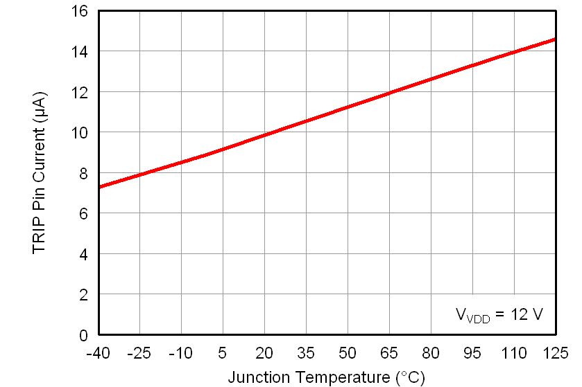 Figure 6-3 TRIP
Pin Current vs Junction Temperature
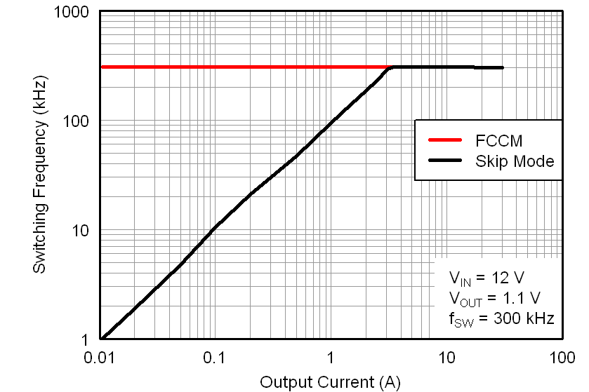 Figure 6-5 Switching Frequency vs Output Current
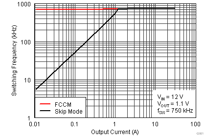 Figure 6-7 Switching Frequency vs Output Current
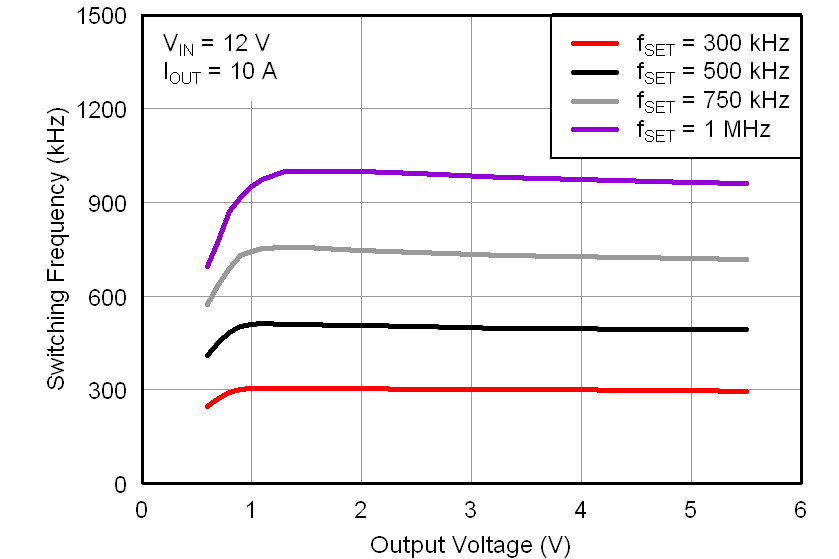 Figure 6-9 Switching Frequency vs Output Voltage
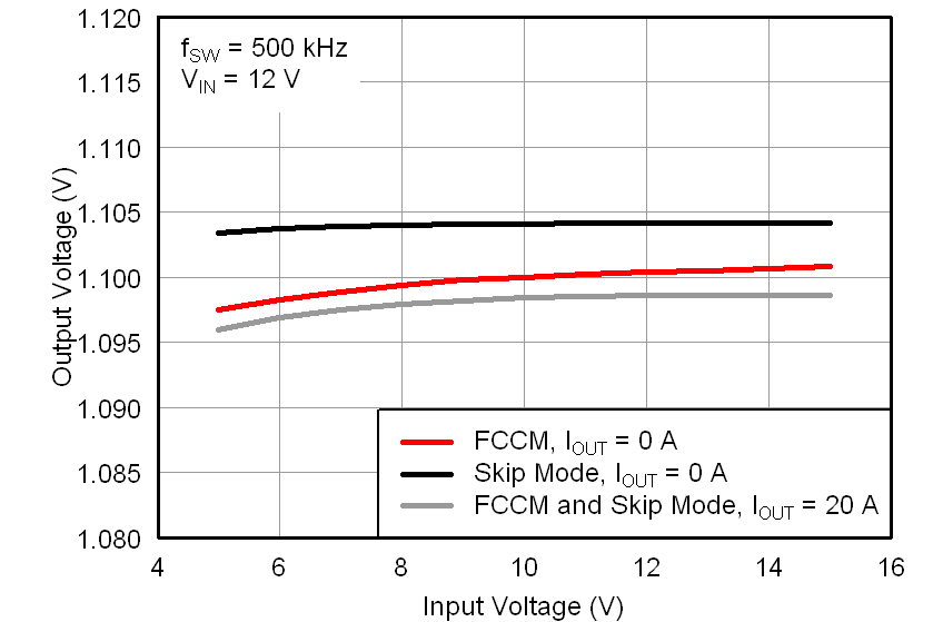 Figure 6-11 Output Voltage vs Input Voltage
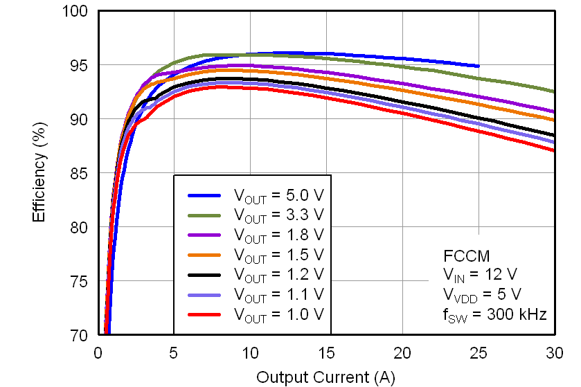 Figure 6-13 Efficiency vs Output Current
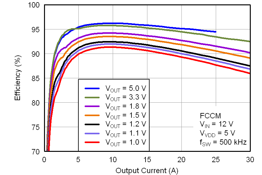 Figure 6-15 Efficiency vs Output Current
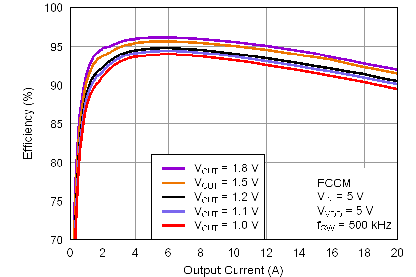 Figure 6-17 Efficiency vs Output Current
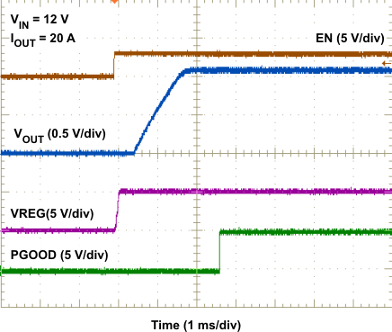 Figure 6-19 Start-Up Waveforms
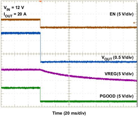 Figure 6-21 Shutdown Waveforms
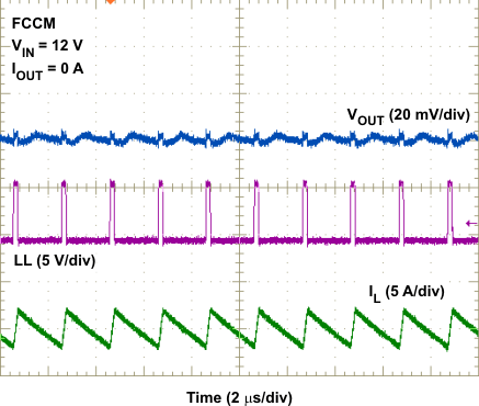 Figure 6-23 1.1-V
Output FCCM Mode Steady-State Operation
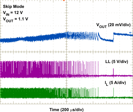 Figure 6-25 CCM
to DCM Transition Waveforms
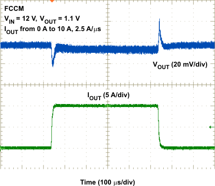 Figure 6-27 FCCM
Load Transient
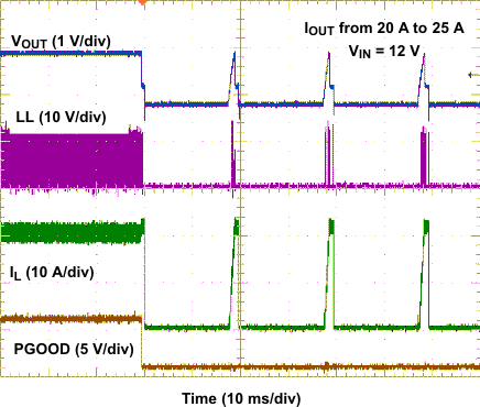 Figure 6-29 Overcurrent Protection Waveforms
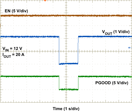 Figure 6-31 Over-temperature Protection Waveforms
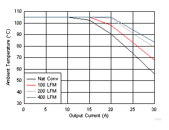
| VIN = 12 V | VOUT = 5 V | fSW = 500 kHz |
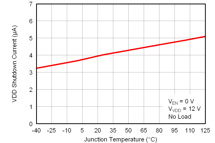 Figure 6-2 VDD
Shutdown Current vs Junction Temperature
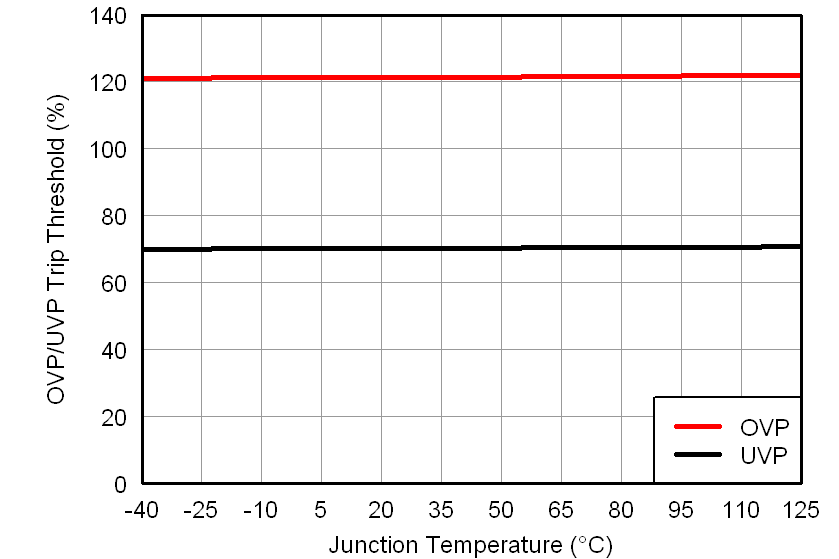 Figure 6-4 OVP/UVP Trip Threshold vs Junction Temperature
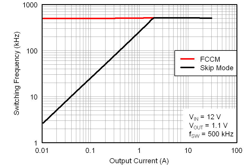 Figure 6-6 Switching Frequency vs Output Current
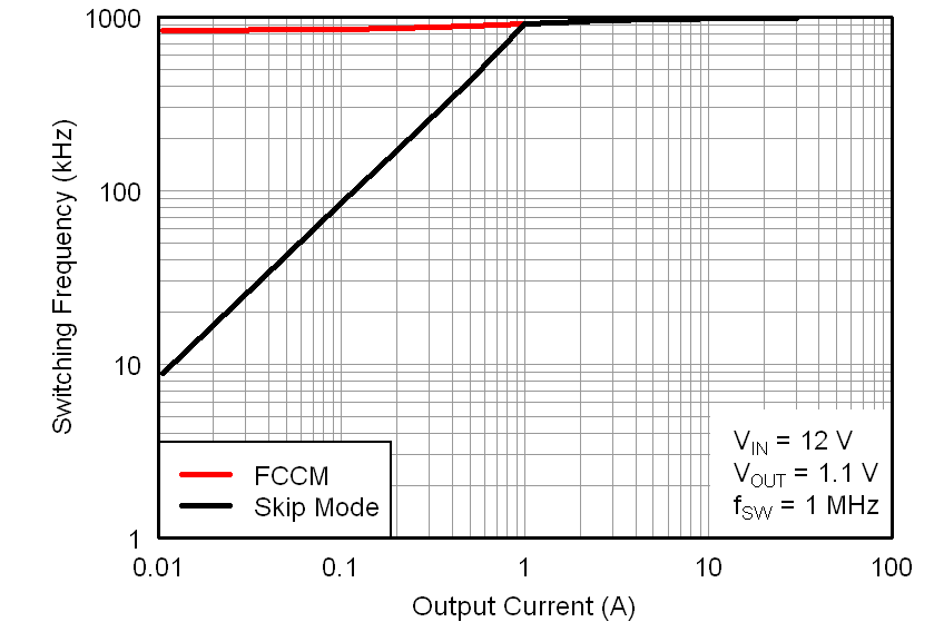 Figure 6-8 Switching Frequency vs Output Current
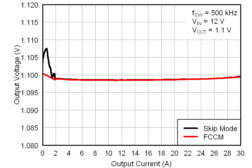 Figure 6-10 Output Voltage vs Output Current
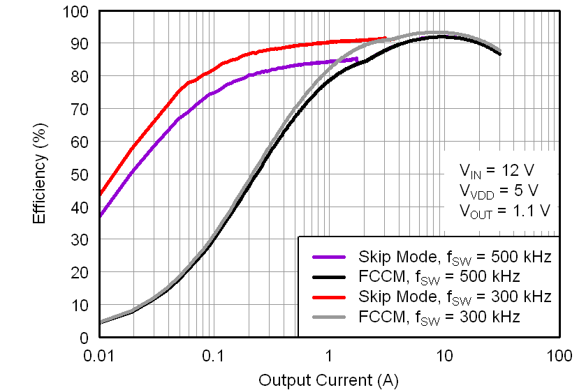 Figure 6-12 Efficiency vs Output Current
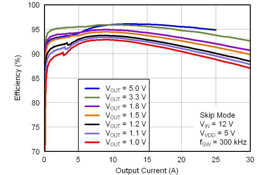 Figure 6-14 Efficiency vs Output Current
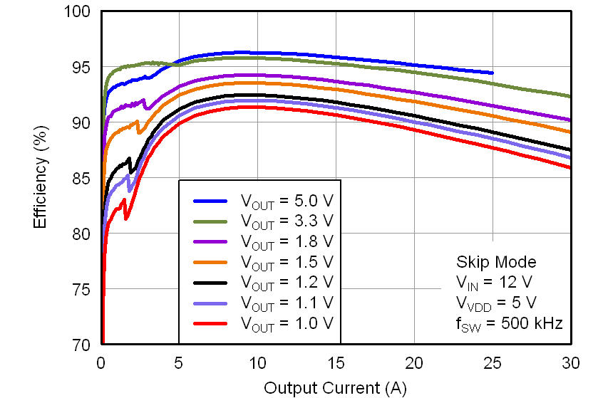 Figure 6-16 Efficiency vs Output Current
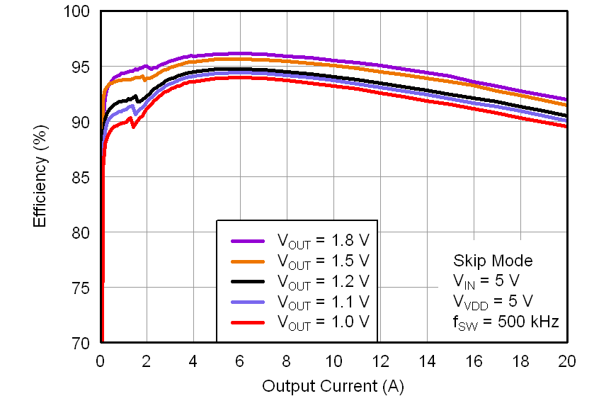 Figure 6-18 Efficiency vs Output Current
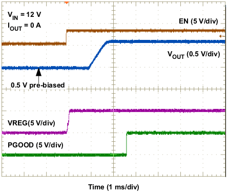 Figure 6-20 Pre-Bias Start-Up Waveforms
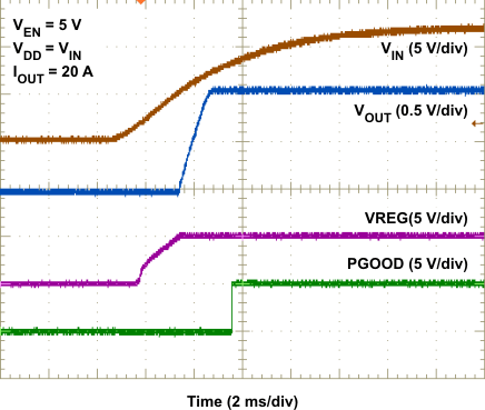 Figure 6-22 UVLO
Start-Up Waveforms
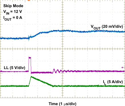 Figure 6-24 1.1-V
Output Skip Mode Steady-State Operation
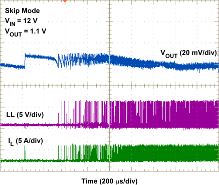 Figure 6-26 DCM
to CCM Transition Waveforms
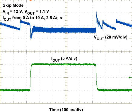 Figure 6-28 Skip
Mode Load Transeint
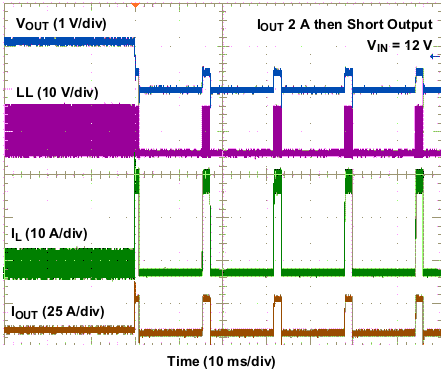 Figure 6-30 Output Short Circuit Protection Waveforms
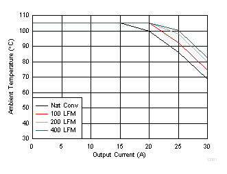
| VIN = 12 V | VOUT = 1.2 V | fSW = 500 kHz |