ZHCS490B November   2011  – December 2018 TMP104

PRODUCTION DATA.  

  1. 1特性
  2. 2应用
  3. 3说明
    1.     Device Images
      1.      典型应用
  4. 4修订历史记录
  5. 5Pin Configuration and Functions
    1.     Pin Functions
  6. 6Specifications
    1. 6.1 Absolute Maximum Ratings
    2. 6.2 ESD Ratings
    3. 6.3 Thermal Information
    4. 6.4 Electrical Characteristics
    5. 6.5 Typical Characteristics
  7. 7Detailed Description
    1. 7.1 Overview
    2. 7.2 Feature Description
      1. 7.2.1 Timeout Function
      2. 7.2.2 Noise
      3. 7.2.3 SMAART Wire™ Interface Timing Specifications
    3. 7.3 Programming
      1. 7.3.1 Communication Protocol
      2. 7.3.2 Command Register
      3. 7.3.3 Global Initialization and Address Assignment Sequence
      4. 7.3.4 Global Read and Write
      5. 7.3.5 Global Clear Interrupt
      6. 7.3.6 Global Software Reset
      7. 7.3.7 Individual Read and Write
    4. 7.4 Register Maps
      1. 7.4.1 Temperature Register
      2. 7.4.2 Configuration Register
        1. 7.4.2.1 Temperature Watchdog Function (FH, FL)
        2. 7.4.2.2 Conversion Rate (CR1, CR0)
        3. 7.4.2.3 Conversion Modes
          1. 7.4.2.3.1 Shutdown Mode (M1 = 0, M0 = 0)
          2. 7.4.2.3.2 One-Shot Mode (M1 = 0, M0 = 1)
          3. 7.4.2.3.3 Continuous Conversion Mode (M1 = 1)
        4. 7.4.2.4 Interrupt Functionality (INT_EN)
      3. 7.4.3 Temperature Limit Registers
  8. 8器件和文档支持
    1. 8.1 接收文档更新通知
    2. 8.2 社区资源
    3. 8.3 商标
    4. 8.4 静电放电警告
    5. 8.5 术语表
  9. 9机械、封装和可订购信息

封装选项

请参考 PDF 数据表获取器件具体的封装图。

机械数据 (封装 | 引脚)
  • YFF|4
散热焊盘机械数据 (封装 | 引脚)
订购信息

Command Register

Figure 8 shows the internal register structure of the TMP104. Communications between the registers are transferred through the interface in LSB-first order. The 8-bit Command Register, as shown in Table 3, is used to determine the type of instruction being addressed. These eight bits could either interpret a global instruction or an individual instruction, which is determined by the value of P7. When P7 = 0, the command byte interprets an individual instruction; when P7 = 1, the command byte interprets a global instruction.
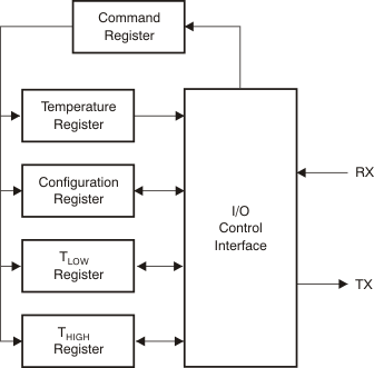
TMP104 ai_internal_register_bos564.gifFigure 8. Internal Register Structure

Table 3. Command Register Byte

P7 P6 P5 P4 P3 P2 P1 P0
GLB IN3/ID3 IN2/ID2 IN1/ID1 IN0/ID0 P1 P0 R/W