ZHCS227G June 2011 – April 2024 LP2951-Q1
PRODUCTION DATA
- 1
- 1 特性
- 2 应用
- 3 说明
- 4 Pin Configuration and Functions
- 5 Specifications
- 6 Detailed Description
- 7 Application and Implementation
- 8 Device and Documentation Support
- 9 Revision History
- 10Mechanical, Packaging, and Orderable Information
封装选项
机械数据 (封装 | 引脚)
散热焊盘机械数据 (封装 | 引脚)
- DRG|8
订购信息
6.3.2 Programming Output Voltage
A unique feature of the LP2951-Q1 is the ability to output either a fixed voltage or an adjustable voltage, depending on the external pin connections. To output the internally programmed fixed voltage, tie the SENSE pin to the OUTPUT pin and the FEEDBACK pin to the VTAP pin. Alternatively, a user-programmable voltage ranging from the internal 1.235-V reference to a 30-V max can be set by using an external resistor divider pair. The resistor divider is tied to VOUT, and the divided-down voltage is tied directly to FEEDBACK for comparison against the internal 1.235-V reference. To satisfy the steady-state condition in which the two inputs are equal, the error amplifier drives the output to equal Equation 1:
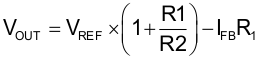
where:
- VREF = 1.235 V applied across R2 (see Figure 6-2)
- IFB = FEEDBACK bias current, typically 20 nA
A minimum regulator output current of 1 μA must be maintained. Thus, in an application where a no-load condition is expected (for example, CMOS circuits in standby), this 1-μA minimum current must be provided by the resistor pair, effectively imposing a maximum value of R2 = 1.2 MΩ (1.235 V / 1.2 MΩ ≉ 1 μA).
IFB = 20 nA introduces an error not approximately equal to 0.02% in VOUT. This error can be offset by trimming R1. Alternatively, increasing the divider current makes IFB less significant, thus, reducing the error contribution. For instance, using R2 = 100 kΩ reduces the error contribution of IFB to 0.17% by increasing the divider current to not approximately equal to 12 μA. This increase in the divider current still is small compared to the 600-μA typical quiescent current of the LP2951-Q1 under no load.
 Figure 6-2 Adjusting
the Feedback on the LP2951-Q1
Figure 6-2 Adjusting
the Feedback on the LP2951-Q1