ZHCS227G June 2011 – April 2024 LP2951-Q1
PRODUCTION DATA
- 1
- 1 特性
- 2 应用
- 3 说明
- 4 Pin Configuration and Functions
- 5 Specifications
- 6 Detailed Description
- 7 Application and Implementation
- 8 Device and Documentation Support
- 9 Revision History
- 10Mechanical, Packaging, and Orderable Information
封装选项
机械数据 (封装 | 引脚)
散热焊盘机械数据 (封装 | 引脚)
- DRG|8
订购信息
6.3.1 ERROR Function
The LP2951-Q1 has a low-voltage detection comparator that outputs a logic low when the output voltage drops by approximately 6% from the nominal value, and outputs a logic high when VOUT has reached approximately 95% of the nominal value. This 95% of nominal figure is obtained by dividing the built-in offset of approximately 60 mV by the 1.235-V band-gap reference, and remains independent of the programmed output voltage. For example, the trip-point threshold (ERROR output goes high) typically is 4.75 V for a 5-V output and 11.4 V for a 12-V output. Typically, there is a hysteresis of 15 mV between the thresholds for a high and low ERROR output.
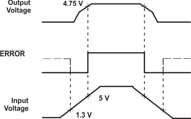
A timing diagram is shown in Figure 6-1 for ERROR vs VOUT (5 V), as VIN is ramped up and down. ERROR becomes valid (low) when VIN is approximately 1.3 V. When VIN is approximately 5 V, VOUT = 4.75 V, causing ERROR to go high. Because the dropout voltage is load dependent, the output trip-point threshold is reached at different values of VIN, depending on the load current. For instance, at higher load current, ERROR goes high at a slightly higher value of VIN, and vice versa for lower load current. The output-voltage trip point remains at approximately 4.75 V, regardless of the load. When VIN ≤ 1.3 V, the ERROR comparator output is turned off and pulled high to the pullup voltage. If VOUT is used as the pullup voltage, rather than an external 5-V source, ERROR typically is approximately 1.2 V. In this condition, an equal resistor divider (10 kΩ is acceptable) can be tied to ERROR to divide down the voltage to a valid logic low during any fault condition, while still enabling a logic high during normal operation.
 Figure 6-1 ERROR Output Timing
Because the ERROR comparator has an open-collector output, an external pullup resistor is required to pull the output up to VOUT or another supply voltage (up to 30 V). The output of the comparator is rated to sink up to 400 μA. An acceptable range of values for the pullup resistor is from 100 kΩ to 1 MΩ. If ERROR is not used, this pin can be left open.