ZHCSJE9I April 2004 – February 2019 LM2743
PRODUCTION DATA.
- 1 特性
- 2 应用
- 3 说明
- 4 修订历史记录
- 5 Pin Configuration and Functions
- 6 Specifications
- 7 Detailed Description
- 8 Application and Implementation
- 9 Power Supply Recommendations
- 10Layout
- 11器件和文档支持
- 12机械、封装和可订购信息
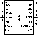
5 Pin Configuration and Functions
PW Package
14-Pin TSSOP
Top View

Pin Functions
| PIN | DESCRIPTION | |
|---|---|---|
| NAME | NO. | |
| BOOT | 1 | Bootstrap pin. This is the supply rail for the gate drivers. When the high-side MOSFET turns on, the voltage on this pin should be at least one gate threshold above the regulator input voltage VIN to properly turn on the MOSFET. See MOSFET Gate Drivers for more details on how to select MOSFETs. |
| LG | 2 | Low-gate drive pin. This is the gate drive for the low-side N-channel MOSFET. This signal is interlocked with the high-side gate drive HG (Pin 14), so as to avoid shoot-through. |
| PGND | 3 | Power ground. This is also the ground for the low-side MOSFET driver. Both the pins must be connected together on the PCB and form a ground plane, which is usually also the system ground. |
| 13 | ||
| SGND | 4 | Signal ground. It should be connected appropriately to the ground plane with due regard to good layout practices in switching power regulator circuits. |
| VCC | 5 | Supply rail for the control sections of the IC. |
| PWGD | 6 | Power Good pin. This is an open drain output, which is typically meant to be connected to VCC or any other low voltage source through a pull-up resistor. Choose the pull-up resistor so that the current going into this pin is kept below 1 mA. For most applications a recommended value for the pull-up resistor is 100 kΩ. The voltage on this pin is thus pulled low under output under-voltage or over-voltage fault conditions and also under input UVLO. |
| ISEN | 7 | Current limit threshold setting pin. This sources a fixed 40 µA current. A resistor of appropriate value should be connected between this pin and the drain of the low-side MOSFET (switch node). |
| EAO | 8 | Output of the error amplifier. The voltage level on this pin is compared with an internally generated ramp signal to determine the duty cycle. This pin is necessary for compensating the control loop. |
| SS/TRACK | 9 | Soft-start and tracking pin. This pin is internally connected to the non-inverting input of the error amplifier during soft-start, and in fact any time the SS/TRACK pin voltage happens to be below the internal reference voltage. For the basic soft-start function, a capacitor of minimum value 1 nF is connected from this pin to ground. To track the rising ramp of another power supply’s output, connect a resistor divider from the output of that supply to this pin as described in Application and Implementation. |
| FB | 10 | Feedback pin. This is the inverting input of the error amplifier, which is used for sensing the output voltage and compensating the control loop. |
| FREQ | 11 | Frequency adjust pin. The switching frequency is set by connecting a resistor of suitable value between this pin and ground. The equation for calculating the exact value is provided in Application and Implementation, but some typical values (rounded up to the nearest standard values) are 324 kΩ for 100 kHz, 97.6 kΩ for 300 kHz, 56.2 kΩ for 500 kHz, 24.9 kΩ for 1 MHz. |
| SD | 12 | IC shutdown pin. Pull this pin to VCC to ensure the IC is enabled. Connect to ground to disable the IC. Under shutdown, both high-side and low-side drives are off. This pin also features a precision threshold for power supply sequencing purposes, as well as a low threshold to ensure minimal quiescent current. |
| HG | 14 | High-gate drive pin. This is the gate drive for the high-side N-channel MOSFET. This signal is interlocked with LG (Pin 2) to avoid shoot-through. |