ZHCSJE9I April   2004  – February 2019 LM2743

PRODUCTION DATA.  

  1. 特性
  2. 应用
  3. 说明
    1.     Device Images
      1.      典型应用图
  4. 修订历史记录
  5. Pin Configuration and Functions
    1.     Pin Functions
  6. Specifications
    1. 6.1 Absolute Maximum Ratings
    2. 6.2 ESD Ratings
    3. 6.3 Recommended Operating Conditions
    4. 6.4 Thermal Information
    5. 6.5 Electrical Characteristics
    6. 6.6 Typical Characteristics
  7. Detailed Description
    1. 7.1 Overview
    2. 7.2 Functional Block Diagram
    3. 7.3 Feature Description
      1. 7.3.1  Start Up and Soft-Start
      2. 7.3.2  Normal Operation
      3. 7.3.3  Tracking a Voltage Level
      4. 7.3.4  Tracking Voltage Slew Rate
      5. 7.3.5  Sequencing
      6. 7.3.6  SD Pin Impedance
      7. 7.3.7  MOSFET Gate Drivers
      8. 7.3.8  Power Good Signal
      9. 7.3.9  UVLO
      10. 7.3.10 Current Limit
      11. 7.3.11 Foldback Current Limit
    4. 7.4 Device Functional Modes
      1. 7.4.1 Shutdown
  8. Application and Implementation
    1. 8.1 Application Information
    2. 8.2 Typical Applications
      1. 8.2.1 Synchronous Buck Converter Typical Application using LM2743
        1. 8.2.1.1 Design Requirements
        2. 8.2.1.2 Detailed Design Procedure
          1. 8.2.1.2.1 Custom Design With WEBENCH® Tools
          2. 8.2.1.2.2 Duty Cycle Calculation
          3. 8.2.1.2.3 Input Capacitor
          4. 8.2.1.2.4 Output Inductor
          5. 8.2.1.2.5 Output Capacitor
          6. 8.2.1.2.6 MOSFETs
          7. 8.2.1.2.7 Support Components
          8. 8.2.1.2.8 Control Loop Compensation
          9. 8.2.1.2.9 Efficiency Calculations
        3. 8.2.1.3 Application Curves
      2. 8.2.2 Example Circuit 1
        1. 8.2.2.1 Design Requirements
        2. 8.2.2.2 Detailed Design Procedure
        3. 8.2.2.3 Bill of Materials
      3. 8.2.3 Example Circuit 2
        1. 8.2.3.1 Design Requirements
        2. 8.2.3.2 Detailed Design Procedure
        3. 8.2.3.3 Bill of Materials
      4. 8.2.4 Example Circuit 3
        1. 8.2.4.1 Design Requirements
        2. 8.2.4.2 Detailed Design Procedure
        3. 8.2.4.3 Bill of Materials
  9. Power Supply Recommendations
  10. 10Layout
    1. 10.1 Layout Guidelines
    2. 10.2 Layout Example
  11. 11器件和文档支持
    1. 11.1 器件支持
      1. 11.1.1 开发支持
        1. 11.1.1.1 使用 WEBENCH® 工具创建定制设计
    2. 11.2 接收文档更新通知
    3. 11.3 社区资源
    4. 11.4 商标
    5. 11.5 静电放电警告
    6. 11.6 术语表
  12. 12机械、封装和可订购信息

封装选项

机械数据 (封装 | 引脚)
散热焊盘机械数据 (封装 | 引脚)
订购信息

Tracking Voltage Slew Rate

The tracking feature can alternatively be used not to make both rails reach regulation at the same time but rather to have similar rise rates (in terms of output dV/dt). This method ensures that the output voltage of the LM2743 always reaches regulation before the output voltage of the master supply. Because the output of the master supply is divided down, in order to track properly the output voltage of the LM2743 must be lower than the voltage of the master supply. In this case, the tracking resistors can be determined based on the following equation:

Equation 5. LM2743 20095209.gif

For the example case of VOUT1 = 5 V and VOUT2 = 1.8 V, with RT1 set to 150 Ω as before, RT2 is calculated from the above equation to be 265 Ω. A timing diagram for the case of equal slew rates is shown in Figure 21.
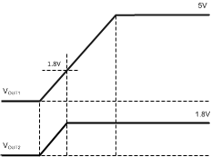
LM2743 20095210.gifFigure 21. Tracking with Equal Slew Rates