ZHCSJE9I April   2004  – February 2019 LM2743

PRODUCTION DATA.  

  1. 特性
  2. 应用
  3. 说明
    1.     Device Images
      1.      典型应用图
  4. 修订历史记录
  5. Pin Configuration and Functions
    1.     Pin Functions
  6. Specifications
    1. 6.1 Absolute Maximum Ratings
    2. 6.2 ESD Ratings
    3. 6.3 Recommended Operating Conditions
    4. 6.4 Thermal Information
    5. 6.5 Electrical Characteristics
    6. 6.6 Typical Characteristics
  7. Detailed Description
    1. 7.1 Overview
    2. 7.2 Functional Block Diagram
    3. 7.3 Feature Description
      1. 7.3.1  Start Up and Soft-Start
      2. 7.3.2  Normal Operation
      3. 7.3.3  Tracking a Voltage Level
      4. 7.3.4  Tracking Voltage Slew Rate
      5. 7.3.5  Sequencing
      6. 7.3.6  SD Pin Impedance
      7. 7.3.7  MOSFET Gate Drivers
      8. 7.3.8  Power Good Signal
      9. 7.3.9  UVLO
      10. 7.3.10 Current Limit
      11. 7.3.11 Foldback Current Limit
    4. 7.4 Device Functional Modes
      1. 7.4.1 Shutdown
  8. Application and Implementation
    1. 8.1 Application Information
    2. 8.2 Typical Applications
      1. 8.2.1 Synchronous Buck Converter Typical Application using LM2743
        1. 8.2.1.1 Design Requirements
        2. 8.2.1.2 Detailed Design Procedure
          1. 8.2.1.2.1 Custom Design With WEBENCH® Tools
          2. 8.2.1.2.2 Duty Cycle Calculation
          3. 8.2.1.2.3 Input Capacitor
          4. 8.2.1.2.4 Output Inductor
          5. 8.2.1.2.5 Output Capacitor
          6. 8.2.1.2.6 MOSFETs
          7. 8.2.1.2.7 Support Components
          8. 8.2.1.2.8 Control Loop Compensation
          9. 8.2.1.2.9 Efficiency Calculations
        3. 8.2.1.3 Application Curves
      2. 8.2.2 Example Circuit 1
        1. 8.2.2.1 Design Requirements
        2. 8.2.2.2 Detailed Design Procedure
        3. 8.2.2.3 Bill of Materials
      3. 8.2.3 Example Circuit 2
        1. 8.2.3.1 Design Requirements
        2. 8.2.3.2 Detailed Design Procedure
        3. 8.2.3.3 Bill of Materials
      4. 8.2.4 Example Circuit 3
        1. 8.2.4.1 Design Requirements
        2. 8.2.4.2 Detailed Design Procedure
        3. 8.2.4.3 Bill of Materials
  9. Power Supply Recommendations
  10. 10Layout
    1. 10.1 Layout Guidelines
    2. 10.2 Layout Example
  11. 11器件和文档支持
    1. 11.1 器件支持
      1. 11.1.1 开发支持
        1. 11.1.1.1 使用 WEBENCH® 工具创建定制设计
    2. 11.2 接收文档更新通知
    3. 11.3 社区资源
    4. 11.4 商标
    5. 11.5 静电放电警告
    6. 11.6 术语表
  12. 12机械、封装和可订购信息

封装选项

机械数据 (封装 | 引脚)
散热焊盘机械数据 (封装 | 引脚)
订购信息

Tracking a Voltage Level

The LM2743 can track the output of a master power supply during soft-start by connecting a resistor divider to the SS/TRACK pin. In this way, the output voltage slew rate of the LM2743 will be controlled by the master supply for loads that require precise sequencing. When the tracking function is used no soft-start capacitor should be connected to the SS/TRACK pin. Otherwise, a CSS value of at least 1 nF between the soft-start pin and ground should be used.
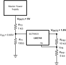
LM2743 20095207.gifFigure 19. Tracking Circuit

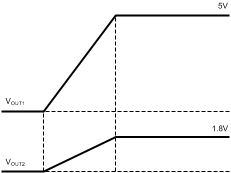
One way to use the tracking feature is to design the tracking resistor divider so that the master supply’s output voltage (VOUT1) and the LM2743’s output voltage (represented symbolically in Figure 19 as VOUT2, that is, without explicitly showing the power components) both rise together and reach their target values at the same time. For this case, the equation governing the values of the tracking divider resistors RT1 and RT2 is:

Equation 4. LM2743 20095218.gif

The current through RT1 should be about 3 mA to 4 mA for precise tracking. The final voltage of the SS/TRACK pin should be set higher than the feedback voltage of 0.6 V (say about 0.65 V as in the above equation). If the master supply voltage was 5 V and the LM2743 output voltage was 1.8 V, for example, then the value of RT1 needed to give the two supplies identical soft-start times would be 150 Ω. A timing diagram for the equal soft-start time case is shown in Figure 20.
LM2743 20095208.gifFigure 20. Tracking with Equal Soft-Start Time