ZHCSJE9I April 2004 – February 2019 LM2743
PRODUCTION DATA.
- 1 特性
- 2 应用
- 3 说明
- 4 修订历史记录
- 5 Pin Configuration and Functions
- 6 Specifications
- 7 Detailed Description
- 8 Application and Implementation
- 9 Power Supply Recommendations
- 10Layout
- 11器件和文档支持
- 12机械、封装和可订购信息
7.3.7 MOSFET Gate Drivers
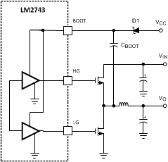
The LM2743 has two gate drivers designed for driving N-channel MOSFETs in a synchronous mode. Note that unlike most other synchronous controllers, the bootstrap capacitor of the LM2743 provides power not only to the driver of the upper MOSFET, but the lower MOSFET driver too (both drivers are ground referenced, i.e. no floating driver). To fully turn the top MOSFET on, the BOOT voltage must be at least one gate threshold greater than VIN when the high-side drive goes high. This bootstrap voltage is usually supplied from a local charge pump structure. But looking at the Typical Application schematic, this also means that the difference voltage VCC - VD1, which is the voltage the bootstrap capacitor charges up to, must be always greater than the maximum tolerance limit of the threshold voltage of the upper MOSFET. Here VD1 is the forward voltage drop across the bootstrap diode D1. This therefore may place restrictions on the minimum input voltage and/or type of MOSFET used.
The most basic charge bootstrap pump circuit can be built using one Schottky diode and a small capacitor, as shown in Figure 25. The capacitor CBOOT serves to maintain enough voltage between the top MOSFET gate and source to control the device even when the top MOSFET is on and its source has risen up to the input voltage level. The charge pump circuitry is fed from VCC, which can operate over a range from 3.0V to 6.0V. Using this basic method the voltage applied to the gates of both high-side and low-side MOSFETs is VCC - VD. This method works well when VCC is 5 V±10%, because the gate drives will get at least 4.0V of drive voltage during the worst case of VCC-MIN = 4.5 V and VD-MAX = 0.5 V. Logic level MOSFETs generally specify their on-resistance at VGS = 4.5 V. When VCC = 3.3 V ±10%, the gate drive at worst case could go as low as 2.5 V. Logic level MOSFETs are not specified to turn on, or may have much higher on-resistance at 2.5 V. Sub-logic level MOSFETs, usually specified at VGS = 2.5 V, will work, but are more expensive, and tend to have higher on-resistance. The circuit in Figure 25 works well for input voltages ranging from 1 V up to 16 V and VCC = 5 V ±10%, because the drive voltage depends only on VCC.
 Figure 25. Basic Charge Pump (Bootstrap)
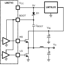
 Note that the LM2743 can be paired with a low cost linear regulator like the LM78L05 to run from a single input rail between 6.0 and 14 V. The 5-V output of the linear regulator powers both the VCC and the bootstrap circuit, providing efficient drive for logic level MOSFETs. An example of this circuit is shown in Figure 26.
 Figure 26. LM78L05 Feeding Basic Charge Pump
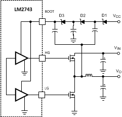
 Figure 27 shows a second possibility for bootstrapping the MOSFET drives using a doubler. This circuit provides an equal voltage drive of VCC - 3VD + VIN to both the high-side and low-side MOSFET drives. This method should only be used in circuits that use 3.3 V for both VCC and VIN. Even with VIN = VCC = 3.0 V (10% lower tolerance on 3.3 V) and VD = 0.5 V both high-side and low-side gates will have at least 4.5 V of drive. The power dissipation of the gate drive circuitry is directly proportional to gate drive voltage, hence the thermal limits of the LM2743 IC will quickly be reached if this circuit is used with VCC or VIN voltages over 5V.
 Figure 27. Charge Pump with Added Gate Drive
 All the gate drive circuits shown in Figure 25 through Figure 27 typically use 100-nF ceramic capacitors in the bootstrap locations.