ZHCSLX3C June 2017 – September 2020 FPC402
PRODUCTION DATA
- 1 特性
- 2 应用
- 3 说明
- 4 Revision History
- 5 说明(续)
- 6 Pin Configuration and Functions
- 7 Specifications
-
8 Detailed Description
- 8.1 Overview
- 8.2 Functional Block Diagram
- 8.3
Feature Description
- 8.3.1 Host-Side Control Interface
- 8.3.2 LED Control
- 8.3.3 Low-Speed Output Signal Control
- 8.3.4 Low-Speed Input Status and Interrupt Generation
- 8.3.5 Downstream (Port-Side) I2C Master
- 8.3.6 Data Prefetch From Modules
- 8.3.7 Scheduled Write
- 8.3.8 Protocol Timeouts
- 8.3.9 General-Purpose Inputs and Outputs
- 8.3.10 Hot-Plug Support
- 8.4 Device Functional Modes
- 8.5 Programming
- 9 Application and Implementation
- 10Power Supply Recommendations
- 11Layout
- 12Device and Documentation Support
- 13Mechanical, Packaging, and Orderable Information
9.2.1 SFP/QSFP Port Management
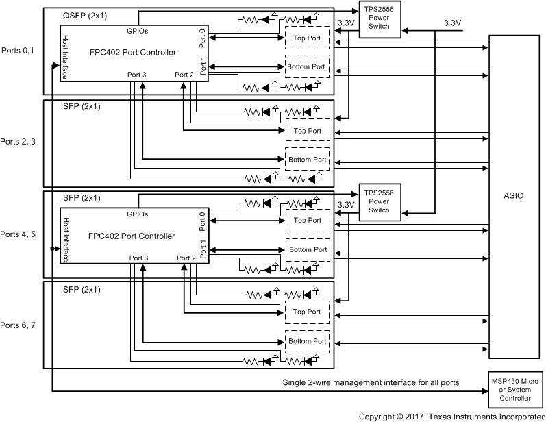
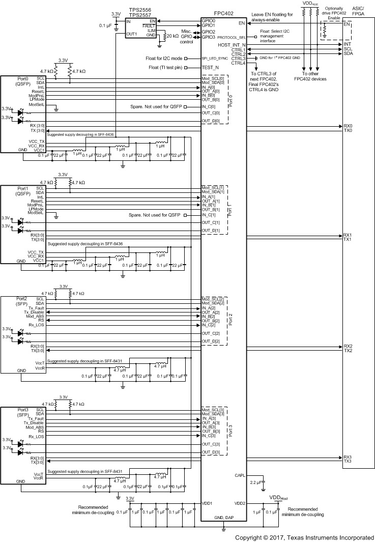
The FPC402 can be used to manage the low-speed signals, I2C, and LEDs for multiple SFP and/or QSFP ports, up to four per FPC402 device. The FPC402 package is optimized to allow placement underneath an SFP or QSFP port on the opposite side of the board. This allows hardware designers to terminate all SFP/QSFP low-speed signals close to the port and route a single I2C or SPI interface back to the system controller (ASIC or FPGA). Figure 9-2 shows an example of this application where two FPC402 devices are used to control two QSFP ports and six SFP ports, in addition to controlling LEDs and two TPS2556 power distribution switches. Figure 9-3 shows an example schematic for the first four ports of this application.
 Figure 9-2 SFP/QSFP Application Block Diagram
 Figure 9-3 SFP/QSFP Application Schematic