ZHCSUH8B December 2017 – January 2024 FPC202
PRODUCTION DATA
- 1
- 1 特性
- 2 应用
- 3 说明
- 4 Device Comparison Table
- 5 Pin Configuration and Functions
- 6 Specifications
-
7 Detailed Description
- 7.1 Overview
- 7.2 Functional Block Diagram
- 7.3
Feature Description
- 7.3.1 Host-Side Control Interface
- 7.3.2 LED Control
- 7.3.3 Low-Speed Output Signal Control
- 7.3.4 Low-Speed Input Status and Interrupt Generation
- 7.3.5 Downstream (Port-Side) I2C Master
- 7.3.6 Data Pre-Fetch From Modules
- 7.3.7 Scheduled Write
- 7.3.8 Protocol Timeouts
- 7.3.9 General-Purpose Inputs/Outputs
- 7.3.10 Hot-Plug Support
- 7.4 Device Functional Modes
- 7.5 Programming
- 8 Application and Implementation
- 9 Device and Documentation Support
- 10Revision History
- 11Mechanical, Packaging, and Orderable Information
8.4.2 Layout Example
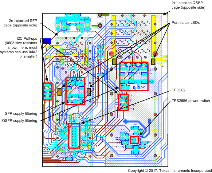
The following layout example shows how the FPC202 can be placed underneath a stacked SFP cage, on the opposite side of the PCB. In this example, the FPC202 is being used to control two SFP ports. For reference, a QSFP footprint, which is wider than the SFP footprint, is shown next to the stacked SFP cage. The FPC202 will also fit beneath a stacked QSFP, QSFP-DD, or OSFP cage. In this example, the FPC202 is using two of its GPIO pins to control a TPS2556 power distribution switch which is placed beneath the QSFP cage. Note that there are multiple ways to route the low-speed control signals and I2C signal between the cages and the FPC202. This example uses two inner layers to accomplish this routing.
 Figure 8-8 Layout Example