ZHCSUH8B December 2017 – January 2024 FPC202
PRODUCTION DATA
- 1
- 1 特性
- 2 应用
- 3 说明
- 4 Device Comparison Table
- 5 Pin Configuration and Functions
- 6 Specifications
-
7 Detailed Description
- 7.1 Overview
- 7.2 Functional Block Diagram
- 7.3
Feature Description
- 7.3.1 Host-Side Control Interface
- 7.3.2 LED Control
- 7.3.3 Low-Speed Output Signal Control
- 7.3.4 Low-Speed Input Status and Interrupt Generation
- 7.3.5 Downstream (Port-Side) I2C Master
- 7.3.6 Data Pre-Fetch From Modules
- 7.3.7 Scheduled Write
- 7.3.8 Protocol Timeouts
- 7.3.9 General-Purpose Inputs/Outputs
- 7.3.10 Hot-Plug Support
- 7.4 Device Functional Modes
- 7.5 Programming
- 8 Application and Implementation
- 9 Device and Documentation Support
- 10Revision History
- 11Mechanical, Packaging, and Orderable Information
7.4.2.1 SPI Frame Structure
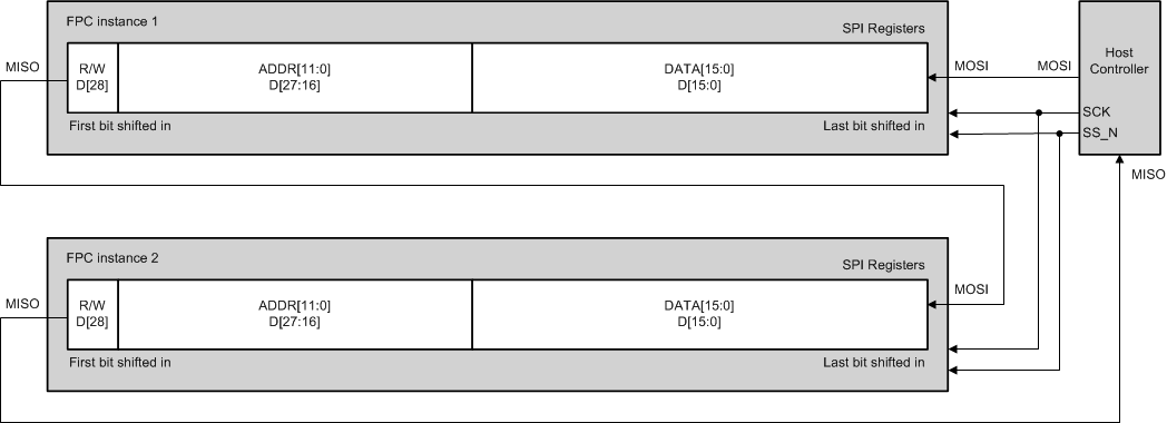
Each SPI transaction to a single FPC202 device is 29 bits long and is framed by the assertion of SS_N (CTRL2) low. The MOSI (CTRL3) input is ignored and the MISO (CTRL4) output is high impedance whenever SS_N is de-asserted high. The prior SPI command, address, and data are shifted out on MISO as the current SPI command, address, and data are shifted in on MOSI. In all SPI transactions, the MISO output signal is enabled asynchronously whenever SS_N is asserted low.
Table 7-8 shows the structure of a SPI frame. Figure 7-7 shows an example implementation, including the internal SPI registers, for two FPC202 devices.
| BIT | FIELD | DESCRIPTION |
|---|---|---|
| 28 | R/W |
0: Write command 1: Read command This is the first bit shifted in on the MOSI input. |
| 27:16 | ADDR[11:0] | 12-bit address field. See Table 7-7. |
| 15 | DATA[15] | Busy flag. For read operations, a '1' means the downstream port is busy. For write operations, DATA[15] is a don't care. |
| 14 | DATA[14] | Don't care. |
| 13 | DATA[13] | NACK received flag. A '1' means the FPC202 has received a NACK from the downstream port. |
| 12 | DATA[12] | Reject flag. A '1' means the FPC202 has rejected the previous command because it is busy servicing a prior command. |
| 11:8 | DATA[11:8] | Don't care. |
| 7:0 | DATA[7:0] |
8-bit data field. DATA[0] is the last bit shifted in on the MOSI input. |
 Figure 7-7 Example SPI Implementation For Two FPC202
Devices
 Figure 7-8 Generic SPI
Transaction
Figure 7-8 Generic SPI
TransactionThe timing specification for an SPI transaction is described in Figure 7-9.
 Figure 7-9 SPI
Timing Diagram