ZHCSUH8B December 2017 – January 2024 FPC202
PRODUCTION DATA
- 1
- 1 特性
- 2 应用
- 3 说明
- 4 Device Comparison Table
- 5 Pin Configuration and Functions
- 6 Specifications
-
7 Detailed Description
- 7.1 Overview
- 7.2 Functional Block Diagram
- 7.3
Feature Description
- 7.3.1 Host-Side Control Interface
- 7.3.2 LED Control
- 7.3.3 Low-Speed Output Signal Control
- 7.3.4 Low-Speed Input Status and Interrupt Generation
- 7.3.5 Downstream (Port-Side) I2C Master
- 7.3.6 Data Pre-Fetch From Modules
- 7.3.7 Scheduled Write
- 7.3.8 Protocol Timeouts
- 7.3.9 General-Purpose Inputs/Outputs
- 7.3.10 Hot-Plug Support
- 7.4 Device Functional Modes
- 7.5 Programming
- 8 Application and Implementation
- 9 Device and Documentation Support
- 10Revision History
- 11Mechanical, Packaging, and Orderable Information
7.3.9 General-Purpose Inputs/Outputs
The FPC202 has multiple general purpose input/output pins which can be used to control auxiliary functions on the board through the same host-side control interface which is used to manage the ports. The GPIO pins can be configured as inputs or outputs through the FPC202 registers. One example use case for these GPIO pins is to control a power switch (for example, TPS2556 or TSP2557) to enable/disable power to the modules in order to manage power sequencing of the modules and prevent large inrush current at board power-up.
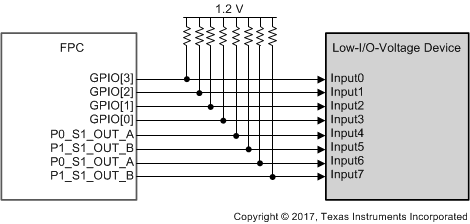
The GPIO pins and other OUT_* pins can be used with an external pull-up resistor to drive low-voltage I/Os on other devices. When used in this fashion, the GPIO/OUT_* pin would drive VOL when set to logic ‘0’, and when set to high-impedance (tri-state), the pull-up resistor would pull the signal up to the appropriate I/O voltage. When using the GPIO/OUT_* pins for this purpose, it is important to drive logic ‘0’ and high-impedance only. Do not drive the pin to logic ‘1’ as it would risk damaging the I/O of the connected device.
Figure 7-3 shows an example configuration for using the GPIOs/OUT_* pins to drive 1.2-V I/Os on another device.
 Figure 7-3 Example Use Of External Pull-Ups to Drive Low-I/O-Voltage Devices
The GPIO pins have a driver impedance of 10 Ω (typical). This is lower than the typical characteristic impedance of a transmission line and therefore may cause ringing due to the fast edge rate. The ringing duration is a function of the transmission line length and will typically be less than 100 ns. The magnitude of the overshoot is a function of the difference of driver impedance and impedance seen by the driver and may be as large as 5 V to GND for a transmission line with a characteristic impedance of 60 Ω. If ringing is a concern, a series resistor may be placed near the GPIO pin. A good rule of thumb for sizing the resistor is the difference of the transmission line characteristic impedance minus the driver impedance. For example, in the case of a 60 Ω transmission line impedance, a 50 Ω series resistor may be used to minimize ringing. Cases such as these may be simulated using the provided FPC202 IBIS model.