ZHCSCL7C May   2014  – April 2021 AFE4403

PRODUCTION DATA  

  1. 特性
  2. 应用
  3. 说明
  4. Revision History
  5. Device Family Options
  6. Pin Configuration and Functions
  7. Specifications
    1. 7.1 Absolute Maximum Ratings
    2. 7.2 ESD Ratings
    3. 7.3 Recommended Operating Conditions
    4. 7.4 Thermal Information
    5. 7.5 Electrical Characteristics
    6. 7.6 Timing Requirements
    7. 7.7 Timing Requirements: Supply Ramp and Power-Down
    8. 7.8 Typical Characteristics
  8. Detailed Description
    1. 8.1 Overview
    2. 8.2 Functional Block Diagram
    3. 8.3 Feature Description
      1. 8.3.1 Receiver Channel
        1. 8.3.1.1 Receiver Front-End
        2. 8.3.1.2 Ambient Cancellation Scheme and Second Stage Gain Block
        3. 8.3.1.3 Receiver Control Signals
        4. 8.3.1.4 Receiver Timing
      2. 8.3.2 Clocking and Timing Signal Generation
      3. 8.3.3 Timer Module
        1. 8.3.3.1 Using the Timer Module
      4. 8.3.4 Receiver Subsystem Power Path
      5. 8.3.5 Transmit Section
        1. 8.3.5.1 Third LED Support
        2. 8.3.5.2 Transmitter Power Path
        3. 8.3.5.3 LED Power Reduction During Periods of Inactivity
        4. 8.3.5.4 LED Configurations
    4. 8.4 Device Functional Modes
      1. 8.4.1 ADC Operation and Averaging Module
        1. 8.4.1.1 Operation Without Averaging
        2. 8.4.1.2 Operation With Averaging
        3. 8.4.1.3 Dynamic Power-Down Mode
      2. 8.4.2 Diagnostics
        1. 8.4.2.1 Photodiode-Side Fault Detection
        2. 8.4.2.2 Transmitter-Side Fault Detection
        3. 8.4.2.3 Diagnostics Module
    5. 8.5 Programming
      1. 8.5.1 Serial Programming Interface
      2. 8.5.2 Reading and Writing Data
        1. 8.5.2.1 Writing Data
        2. 8.5.2.2 Reading Data
        3. 8.5.2.3 Multiple Data Reads and Writes
        4. 8.5.2.4 Register Initialization
        5. 8.5.2.5 AFE SPI Interface Design Considerations
    6. 8.6 Register Maps
      1. 8.6.1 AFE Register Map
      2. 8.6.2 AFE Register Description
  9. Application Information Disclaimer
    1. 9.1 Application Information
    2. 9.2 Typical Application
      1. 9.2.1 Design Requirements
      2. 9.2.2 Detailed Design Procedure
      3. 9.2.3 Application Curves
  10. 10Power Supply Recommendations
    1. 10.1 Power Consumption Considerations
  11. 11Layout
    1. 11.1 Layout Guidelines
    2. 11.2 Layout Example
  12. 12Device and Documentation Support
    1. 12.1 Trademarks
    2. 12.2 静电放电警告
    3. 12.3 术语表
  13. 13Mechanical, Packaging, and Orderable Information

封装选项

机械数据 (封装 | 引脚)
散热焊盘机械数据 (封装 | 引脚)
订购信息

Ambient Cancellation Scheme and Second Stage Gain Block

The receiver provides digital samples corresponding to ambient duration. The host processor (external to the AFE) can use these ambient values to estimate the amount of ambient light leakage. The processor must then set the value of the ambient cancellation DAC using the SPI, as shown in Figure 8-4.

GUID-6844EEF1-EC06-4A4E-8F3D-B548CFF79433-low.gifFigure 8-4 Ambient Cancellation Loop (Closed by the Host Processor)

Using the set value, the ambient cancellation stage subtracts the ambient component and gains up only the pleth component of the received signal; see Figure 8-5. The amplifier gain is programmable to 0 dB, 3.5 dB, 6 dB,
9.5 dB, and 12 dB.

GUID-5995A90B-6743-4E0E-BEA3-25DA13A02C68-low.gifFigure 8-5 Front-End (I-V Amplifier and Cancellation Stage)

The differential output of the second stage is VDIFF, as given by Equation 3:
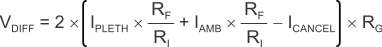
Equation 3. GUID-87D3A605-5EEB-4F36-A5A6-B2557B4AF381-low.gif

where:

  • RI = 100 kΩ,
  • IPLETH = photodiode current pleth component,
  • IAMB = photodiode current ambient component, and
  • ICANCEL = the cancellation current DAC value (as estimated by the host processor).

RG values with various gain settings are listed in Table 8-1.

Table 8-1 RG Values
GAIN RG(kΩ)
0 (x1) 100
3.5 (x1.5) 150
6 (x2) 200
9.5 (x3) 300
12 (x4) 400