ZHCSCL7C May 2014 – April 2021 AFE4403
PRODUCTION DATA
- 1 特性
- 2 应用
- 3 说明
- 4 Revision History
- 5 Device Family Options
- 6 Pin Configuration and Functions
- 7 Specifications
- 8 Detailed Description
- 9 Application Information Disclaimer
- 10Power Supply Recommendations
- 11Layout
- 12Device and Documentation Support
- 13Mechanical, Packaging, and Orderable Information
8.3.2 Clocking and Timing Signal Generation
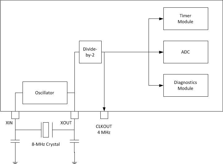
The crystal oscillator generates a master clock signal using an external crystal. In the default mode, a divide-by-2 block converts the 8-MHz clock to 4 MHz, which is used by the AFE to operate the timer modules, ADC, and diagnostics. The 4-MHz clock is buffered and output from the AFE in order to clock an external microcontroller. The clocking functionality is shown in Figure 8-7.
 Figure 8-7 AFE Clocking
To enable flexible clocking, the AFE4403 has a clock divider with programmable division ratios. While the default division ratio is divide-by-2, the clock divider can be programmed to select between ratios of 1, 2, 4, 6, 8, or 12. The division ratio should be selected based on the external clock input frequency such that the divided clock has a frequency close to 4 MHz. For this reason, CLKOUT is referred as a 4-MHz clock in this document. When operating with an external clock input, the divider is reset based on the RESET rising edge. Figure 8-8 shows the case where the divider ratio is set to divide-by-2.
 Figure 8-8 Clock Divider Reset
The device supports both external clock mode as well as an internal clock mode with external crystal.
In the external clock mode, an external clock is input on the XIN pin and the device internally generates the internal clock (used by the timing engine and the ADC) by a programmable division ratio. After division, the internal clock should be within a range of 4 MHz to 6 MHz. The exact frequency of this divided clock is one of the pieces of information required to establish the heart rate being measured from the pulse data.
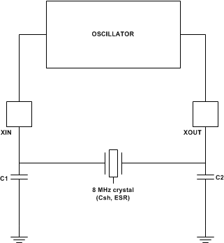
In internal clock mode, an external crystal (connected between XIN and XOUT) is used to generate the clock. To generate sustained oscillations, the oscillator within the AFE provides negative resistance to cancel out the ESR of the crystal. A good rule of thumb is to limit the ESR of the crystal to less than a third of the negative resistance achievable by the oscillator. Figure 8-9 shows the connection of Crystal to AFE4403.
 Figure 8-9 Connection of Crystal to AFE4403
In Figure 8-9 the crystal is characterized by a capacitance, Csh (shunt capacitance of the crystal) and an equivalent series resistance (ESR). C1 and C2 are external capacitors added at the XIN and XOUT pins.
The negative resistance achievable from the internal oscillator is given by Equation 4:
where
- CL = (C1 × C2) / (C1 + C2),
- ω is the frequency of oscillation in rads,
- Csh is the shunt capacitor of the crystal, and
- C1, C2 are the capacitors to ground from the XIN, XOUT pins. A value of approximately 15 pF is recommended for C1, C2.
For example, with Csh = 8 pF, C1 = C2 = 15 pF, and a frequency of 8 MHz, the result is Equation 5:
Thus, the crystal ESR is limited to less than approximately 200 Ω.
TI highly recommends that a single clock source be used to generate the clock required by the AFE as well as the clock needed by the microcontroller (MCU). If an independent clock source is used by the MCU, then any energy coupling into the AFE supply or ground or input pins can cause aliased spurious tones close to the heart rate being measured. To enable operation with the single clock source between the AFE and the MCU, two options are possible:
- AFE clock as master: The AFE uses a crystal to generate its clock. CLKOUT from the AFE is used as the input clock for the MCU.
- MCU clock as master: The AFE operates with an external clock provided by the MCU.
Note that the switching of CLKOUT consumes power. Thus, if CLKOUT is not used, it can be shut off using the CLKOUT_TRI bit.