ZHCSCL7C May 2014 – April 2021 AFE4403
PRODUCTION DATA
- 1 特性
- 2 应用
- 3 说明
- 4 Revision History
- 5 Device Family Options
- 6 Pin Configuration and Functions
- 7 Specifications
- 8 Detailed Description
- 9 Application Information Disclaimer
- 10Power Supply Recommendations
- 11Layout
- 12Device and Documentation Support
- 13Mechanical, Packaging, and Orderable Information
8.4.1.3 Dynamic Power-Down Mode
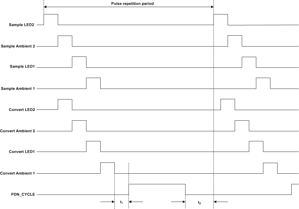
When operated at low PRF, a dynamic power-down mode can be optionally enabled to shut off blocks during a portion of each period. This operation is illustrated in Figure 8-30. The dynamic power-down signal (called PDN_CYCLE) can be internally generated using the timing controller. PDN_CYCLE can be used to shut off power to internal blocks during the unused section within each pulse repetition period.
 Figure 8-30 Dynamic
Power-Down Mode Timing
Figure 8-30 Dynamic
Power-Down Mode Timingt1 and t2 denote the timing margin between the active portion of the period and the dynamic power-down signal. TI recommends setting t1 > 50 µs and t2 > 200 µs in order to ensure sufficient time for the shutdown blocks to recover from power-down. By choosing the blocks that are shut down during dynamic power-down, a power savings of anywhere between 35% to 70% power can be achieved when the PDN_CYCLE phase is active.
The sequence of the convert phases within a pulse repetition period should be as follows: LED2 (Red) → Ambient 2 → LED1 (IR) → Ambient 1. The sample phases must precede the corresponding convert phase. Also note that the ADC_RDY signal coincides with the first ADC Reset signal. The time window between the ADC_RDY (first ADC Reset) and the second ADC Reset represents the window where the contents of all the 6 registers correspond to the samples of the four conversion phases from the previous pulse repetition period.
The MCU could either read all of these registers during this time window, or could read each register separately in the time window where its contents are stable.
The DYNAMIC1, DYNAMIC2, DYNAMIC3, and DYNAMIC4 bits determine which blocks are powered down during the dynamic power-down state (when PDN_CYCLE is high). For maximum power saving, all four bits can be set to 1. TI recommends setting t1 to greater than 100 µs and t2 to greater than 200 µs to ensure that the blocks recover from power-down in time for the next cycle.
The bit corresponding to the TIA power-down (DYNAMIC3) needs a bit more consideration. When the TIA is powered down, the TIA no longer maintains the bias across the photodiode output. This loss of bias can cause the photodiode output voltage to drift from the normal value. The recovery time constant associated with the photodiode returning to a proper bias condition (when the TIA is powered back on) is approximately equal to 2 × CPD × RF, where CPD is the effective differential capacitance of the photodiode and RF is the TIA gain setting. This consideration might result in a different choice for the value of t2.