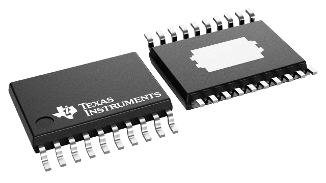
封装信息
| 封装 | 引脚 HTSSOP (PWP) | 20 |
| 工作温度范围 (°C) -55 to 125 |
| 包装数量 | 包装 2,000 | LARGE T&R |
TPS70751-EP 的特性
- Controlled Baseline
- One Assembly/Test Site, One Fabrication Site
- Enhanced Diminishing Manufacturing Sources (DMS) Support
- Enhanced Product-Change Notification
- Qualification Pedigree(1)
- Dual Output Voltages for Split-Supply Applications
- Selectable Power-Up Sequencing for DSP Applications (See Part Number TPS708xx for Independently Enabled Outputs)
- Output Current Range of 250 mA on Regulator 1 and 125 mA on Regulator 2
- Fast Transient Response
- 3.3-V/1.8-V Fixed Voltage Outputs
- Open-Drain Power-On Reset With 120-ms Delay
- Open-Drain Power Good for Regulator 1
- Ultralow 190-µA (Typ) Quiescent Current
- 1-µA Input Current During Standby
- Low Noise: 65 µVrms Without Bypass Capacitor
- Quick Output Capacitor Discharge Feature
- Two Manual Reset Inputs
- 2% Accuracy Over Load and Temperature
- Undervoltage Lockout (UVLO) Feature
- 20-Pin PowerPAD™ Thin Shrink Small-Outline Package (TSSOP)
- Thermal Shutdown Protection
PowerPAD Is a trademark of Texas Instruments
(1) Component qualification in accordance with JEDEC and industry standards to ensure reliable operation over an extended temperature range. This includes, but is not limited to, Highly Accelerated Stress Test (HAST) or biased 85/85, temperature cycle, autoclave or unbiased HAST, electromigration, bond intermetallic life, and mold compound life. Such qualification testing should not be viewed as justifying use of this component beyond specified performance and environmental limits.
TPS70751-EP 的说明
The TPS707xx family devices are designed to provide a complete power-management solution for TI DSP, processor power, ASIC, FPGA, and digital applications where dual-output voltage regulators are required. Easy programmability of the sequencing function makes this family ideal for any TI DSP applications with power-sequencing requirements. Differentiated features, such as accuracy, fast transient response, SVS supervisory circuit (power-on reset), manual reset inputs, and enable function, provide a complete system solution.
The TPS707xx family of voltage regulators offer very low dropout (LDO) voltage and dual outputs with power-up sequence control, which is designed primarily for DSP applications. These devices have extremely low noise output performance without using any added filter bypass capacitors, and are designed to have a fast transient response and be stable with 10-µF low ESR capacitors.
The TPS70751 has a fixed voltage of 3.3 V/1.8 V. Regulator 1 can support up to 250 mA and regulator 2 can support up to 125 mA. Separate voltage inputs allow the designer to configure the source power.
Because the PMOS device behaves as a low-value resistor, the dropout voltage is very low (typically 83 mV on regulator 1) and is directly proportional to the output current. Additionally, since the PMOS pass element is a voltage-driven device, the quiescent current is very low and independent of output loading (maximum of 230 µA over the full range of output current). This LDO family also features a sleep mode; applying a high signal to EN (enable) shuts down both regulators, reducing the input current to 1 µA at TJ = 25°C.
The device is enabled when the enable (EN) pin is connected to a low-level input voltage. The output voltages of the two regulators are sensed at the VSENSE1 and VSENSE2 pins, respectively.
The input signal at the sequence (SEQ) pin controls the power-up sequence of the two regulators. When the device is enabled and SEQ is pulled high or left open, VOUT2 turns on first and VOUT1 remains off until VOUT2 reaches approximately 83% of its regulated output voltage. At that time, VOUT1 is turned on. If VOUT2 is pulled below 83% (i.e., overload condition), VOUT1 is turned off. Pulling SEQ low reverses the power-up order and VOUT1 is turned on first. SEQ is connected to an internal pullup current source.
For each regulator, there is an internal discharge transistor to discharge the output capacitor when the regulator is turned off (disabled).
The power good (PG1) pin reports the voltage conditions at VOUT1. Power good can be used to implement a SVS for the circuitry supplied by regulator 1.
The TPS70751 features a RESET (SVS, POR, or power-on reset). The RESET output initiates a reset in DSP systems and related digital applications in the event of an undervoltage condition. RESET indicates the status of VOUT2 and both manual reset (MR1 and MR2) pins. When VOUT2 reaches 95% of its regulated voltage and MR1 and MR2 are in the logic high state, RESET goes to a high-impedance state after a 120-ms delay. RESET goes to logic low state when VOUT2 regulated output voltage is pulled below 95% (i.e., overload condition) of its regulated voltage. To monitor VOUT1, the PG1 output can be connected to MR1 or MR2.
The device has an undervoltage lockout (UVLO) circuit that prevents the internal regulators from turning on until VIN1 reaches 2.5 V.
