ZHCSNG8B February   2021  – September 2022 CC2652RSIP

PRODUCTION DATA  

  1. 特性
  2. 应用
  3. 说明
  4. Functional Block Diagram
  5. Revision History
  6. Device Comparison
  7. Terminal Configuration and Functions
    1. 7.1 Pin Diagram
    2. 7.2 Signal Descriptions – SIP Package
    3. 7.3 Connections for Unused Pins and Modules
  8. Specifications
    1. 8.1  Absolute Maximum Ratings
    2. 8.2  ESD Ratings
    3. 8.3  Recommended Operating Conditions
    4. 8.4  Power Supply and Modules
    5. 8.5  Power Consumption - Power Modes
    6. 8.6  Power Consumption - Radio Modes
    7. 8.7  Nonvolatile (Flash) Memory Characteristics
    8. 8.8  Thermal Resistance Characteristics
    9. 8.9  RF Frequency Bands
    10. 8.10 Bluetooth Low Energy - Receive (RX)
    11. 8.11 Bluetooth Low Energy - Transmit (TX)
    12. 8.12 Zigbee and Thread - IEEE 802.15.4-2006 2.4 GHz (OQPSK DSSS1:8, 250 kbps) - RX
    13. 8.13 Zigbee and Thread - IEEE 802.15.4-2006 2.4 GHz (OQPSK DSSS1:8, 250 kbps) - TX
    14. 8.14 Timing and Switching Characteristics
      1. 8.14.1 Reset Timing
      2. 8.14.2 Wakeup Timing
      3. 8.14.3 Clock Specifications
        1. 8.14.3.1 48 MHz Crystal Oscillator (XOSC_HF)
        2. 8.14.3.2 48 MHz RC Oscillator (RCOSC_HF)
        3. 8.14.3.3 2 MHz RC Oscillator (RCOSC_MF)
        4. 8.14.3.4 32.768 kHz Crystal Oscillator (XOSC_LF)
        5. 8.14.3.5 32 kHz RC Oscillator (RCOSC_LF)
      4. 8.14.4 Synchronous Serial Interface (SSI) Characteristics
        1. 8.14.4.1 Synchronous Serial Interface (SSI) Characteristics
        2.       36
      5. 8.14.5 UART
        1.       38
    15. 8.15 Peripheral Characteristics
      1. 8.15.1 ADC
        1.       Analog-to-Digital Converter (ADC) Characteristics
      2. 8.15.2 DAC
        1. 8.15.2.1 Digital-to-Analog Converter (DAC) Characteristics
      3. 8.15.3 Temperature and Battery Monitor
        1. 8.15.3.1 Temperature Sensor
        2. 8.15.3.2 Battery Monitor
      4. 8.15.4 Comparators
        1. 8.15.4.1 Low-Power Clocked Comparator
        2. 8.15.4.2 Continuous Time Comparator
      5. 8.15.5 Current Source
        1. 8.15.5.1 Programmable Current Source
      6. 8.15.6 GPIO
        1. 8.15.6.1 GPIO DC Characteristics
    16. 8.16 Typical Characteristics
      1. 8.16.1 MCU Current
      2. 8.16.2 RX Current
      3. 8.16.3 TX Current
      4. 8.16.4 RX Performance
      5. 8.16.5 TX Performance
      6. 8.16.6 ADC Performance
  9. Detailed Description
    1. 9.1  Overview
    2. 9.2  System CPU
    3. 9.3  Radio (RF Core)
      1. 9.3.1 Bluetooth 5.2 Low Energy
      2. 9.3.2 802.15.4 (Thread, Zigbee, 6LoWPAN)
    4. 9.4  Memory
    5. 9.5  Sensor Controller
    6. 9.6  Cryptography
    7. 9.7  Timers
    8. 9.8  Serial Peripherals and I/O
    9. 9.9  Battery and Temperature Monitor
    10. 9.10 µDMA
    11. 9.11 Debug
    12. 9.12 Power Management
    13. 9.13 Clock Systems
    14. 9.14 Network Processor
    15. 9.15 Device Certification and Qualification
      1. 9.15.1 FCC Certification and Statement
      2. 9.15.2 IC/ISED Certification and Statement
      3. 9.15.3 ETSI/CE Certification
      4. 9.15.4 UK Certification
    16. 9.16 Module Markings
    17. 9.17 End Product Labeling
    18. 9.18 Manual Information to the End User
  10. 10Application, Implementation, and Layout
    1. 10.1 Application Information
      1. 10.1.1 Typical Application Circuit
    2. 10.2 Device Connection and Layout Fundamentals
      1. 10.2.1 Reset
      2. 10.2.2 Unused Pins
    3. 10.3 PCB Layout Guidelines
      1. 10.3.1 General Layout Recommendations
      2. 10.3.2 RF Layout Recommendations
        1. 10.3.2.1 Antenna Placement and Routing
        2. 10.3.2.2 Transmission Line Considerations
    4. 10.4 Reference Designs
    5. 10.5 Junction Temperature Calculation
  11. 11Environmental Requirements and SMT Specifications
    1. 11.1 PCB Bending
    2. 11.2 Handling Environment
      1. 11.2.1 Terminals
      2. 11.2.2 Falling
    3. 11.3 Storage Condition
      1. 11.3.1 Moisture Barrier Bag Before Opened
      2. 11.3.2 Moisture Barrier Bag Open
    4. 11.4 PCB Assembly Guide
      1. 11.4.1 PCB Land Pattern & Thermal Vias
      2. 11.4.2 SMT Assembly Recommendations
      3. 11.4.3 PCB Surface Finish Requirements
      4. 11.4.4 Solder Stencil
      5. 11.4.5 Package Placement
      6. 11.4.6 Solder Joint Inspection
      7. 11.4.7 Rework and Replacement
      8. 11.4.8 Solder Joint Voiding
    5. 11.5 Baking Conditions
    6. 11.6 Soldering and Reflow Condition
  12. 12Device and Documentation Support
    1. 12.1 Device Nomenclature
    2. 12.2 Tools and Software
      1. 12.2.1 SimpleLink™ Microcontroller Platform
    3. 12.3 Documentation Support
    4. 12.4 支持资源
    5. 12.5 Trademarks
    6. 12.6 Electrostatic Discharge Caution
    7. 12.7 术语表
  13. 13Mechanical, Packaging, and Orderable Information
    1. 13.1 Packaging Information

Soldering and Reflow Condition

  • Heating method: Conventional convection or IR convection
  • Temperature measurement: Thermocouple d = 0.1 mm to 0.2 mm CA (K) or CC (T) at soldering portion or equivalent method
  • Solder paste composition: SAC305
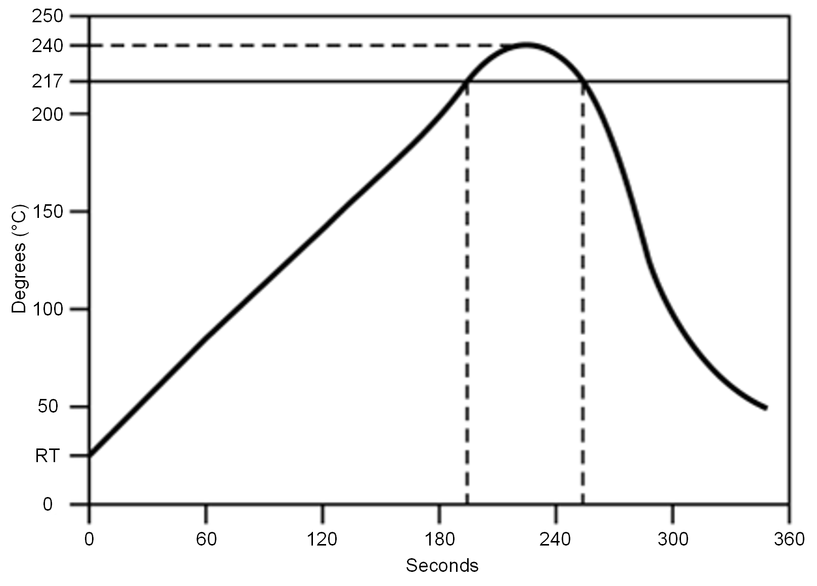
  • Allowable reflow soldering times: 2 times based on the reflow soldering profile (see Figure 11-1)
  • Temperature profile: Reflow soldering will be done according to the temperature profile (see
    Figure 11-1)
  • Peak temperature: 260°C
GUID-EE9AB1EC-1487-44FD-91B0-8B6663289576-low.png Figure 11-1 Temperature Profile for Evaluation of Solder Heat Resistance of a Component (at Solder Joint)
Table 11-1 Temperature Profile
Profile Elements Convection or IR(1)
Peak temperature range 235 to 240°C typical (260°C maximum)
Pre-heat / soaking (150 to 200°C) 60 to 120 seconds
Time above melting point 60 to 90 seconds
Time with 5°C to peak 30 seconds maximum
Ramp up < 3°C / second
Ramp down < -6°C / second
For details, refer to the solder paste manufacturer's recommendation.


Note:

TI does not recommend the use of conformal coating or similar material on the SimpleLink™ module. This coating can lead to localized stress on the solder connections inside the module and impact the module reliability. Use caution during the module assembly process to the final PCB to avoid the presence of foreign material inside the module.