ZHCSNG8B February   2021  – September 2022 CC2652RSIP

PRODUCTION DATA  

  1. 特性
  2. 应用
  3. 说明
  4. Functional Block Diagram
  5. Revision History
  6. Device Comparison
  7. Terminal Configuration and Functions
    1. 7.1 Pin Diagram
    2. 7.2 Signal Descriptions – SIP Package
    3. 7.3 Connections for Unused Pins and Modules
  8. Specifications
    1. 8.1  Absolute Maximum Ratings
    2. 8.2  ESD Ratings
    3. 8.3  Recommended Operating Conditions
    4. 8.4  Power Supply and Modules
    5. 8.5  Power Consumption - Power Modes
    6. 8.6  Power Consumption - Radio Modes
    7. 8.7  Nonvolatile (Flash) Memory Characteristics
    8. 8.8  Thermal Resistance Characteristics
    9. 8.9  RF Frequency Bands
    10. 8.10 Bluetooth Low Energy - Receive (RX)
    11. 8.11 Bluetooth Low Energy - Transmit (TX)
    12. 8.12 Zigbee and Thread - IEEE 802.15.4-2006 2.4 GHz (OQPSK DSSS1:8, 250 kbps) - RX
    13. 8.13 Zigbee and Thread - IEEE 802.15.4-2006 2.4 GHz (OQPSK DSSS1:8, 250 kbps) - TX
    14. 8.14 Timing and Switching Characteristics
      1. 8.14.1 Reset Timing
      2. 8.14.2 Wakeup Timing
      3. 8.14.3 Clock Specifications
        1. 8.14.3.1 48 MHz Crystal Oscillator (XOSC_HF)
        2. 8.14.3.2 48 MHz RC Oscillator (RCOSC_HF)
        3. 8.14.3.3 2 MHz RC Oscillator (RCOSC_MF)
        4. 8.14.3.4 32.768 kHz Crystal Oscillator (XOSC_LF)
        5. 8.14.3.5 32 kHz RC Oscillator (RCOSC_LF)
      4. 8.14.4 Synchronous Serial Interface (SSI) Characteristics
        1. 8.14.4.1 Synchronous Serial Interface (SSI) Characteristics
        2.       36
      5. 8.14.5 UART
        1.       38
    15. 8.15 Peripheral Characteristics
      1. 8.15.1 ADC
        1.       Analog-to-Digital Converter (ADC) Characteristics
      2. 8.15.2 DAC
        1. 8.15.2.1 Digital-to-Analog Converter (DAC) Characteristics
      3. 8.15.3 Temperature and Battery Monitor
        1. 8.15.3.1 Temperature Sensor
        2. 8.15.3.2 Battery Monitor
      4. 8.15.4 Comparators
        1. 8.15.4.1 Low-Power Clocked Comparator
        2. 8.15.4.2 Continuous Time Comparator
      5. 8.15.5 Current Source
        1. 8.15.5.1 Programmable Current Source
      6. 8.15.6 GPIO
        1. 8.15.6.1 GPIO DC Characteristics
    16. 8.16 Typical Characteristics
      1. 8.16.1 MCU Current
      2. 8.16.2 RX Current
      3. 8.16.3 TX Current
      4. 8.16.4 RX Performance
      5. 8.16.5 TX Performance
      6. 8.16.6 ADC Performance
  9. Detailed Description
    1. 9.1  Overview
    2. 9.2  System CPU
    3. 9.3  Radio (RF Core)
      1. 9.3.1 Bluetooth 5.2 Low Energy
      2. 9.3.2 802.15.4 (Thread, Zigbee, 6LoWPAN)
    4. 9.4  Memory
    5. 9.5  Sensor Controller
    6. 9.6  Cryptography
    7. 9.7  Timers
    8. 9.8  Serial Peripherals and I/O
    9. 9.9  Battery and Temperature Monitor
    10. 9.10 µDMA
    11. 9.11 Debug
    12. 9.12 Power Management
    13. 9.13 Clock Systems
    14. 9.14 Network Processor
    15. 9.15 Device Certification and Qualification
      1. 9.15.1 FCC Certification and Statement
      2. 9.15.2 IC/ISED Certification and Statement
      3. 9.15.3 ETSI/CE Certification
      4. 9.15.4 UK Certification
    16. 9.16 Module Markings
    17. 9.17 End Product Labeling
    18. 9.18 Manual Information to the End User
  10. 10Application, Implementation, and Layout
    1. 10.1 Application Information
      1. 10.1.1 Typical Application Circuit
    2. 10.2 Device Connection and Layout Fundamentals
      1. 10.2.1 Reset
      2. 10.2.2 Unused Pins
    3. 10.3 PCB Layout Guidelines
      1. 10.3.1 General Layout Recommendations
      2. 10.3.2 RF Layout Recommendations
        1. 10.3.2.1 Antenna Placement and Routing
        2. 10.3.2.2 Transmission Line Considerations
    4. 10.4 Reference Designs
    5. 10.5 Junction Temperature Calculation
  11. 11Environmental Requirements and SMT Specifications
    1. 11.1 PCB Bending
    2. 11.2 Handling Environment
      1. 11.2.1 Terminals
      2. 11.2.2 Falling
    3. 11.3 Storage Condition
      1. 11.3.1 Moisture Barrier Bag Before Opened
      2. 11.3.2 Moisture Barrier Bag Open
    4. 11.4 PCB Assembly Guide
      1. 11.4.1 PCB Land Pattern & Thermal Vias
      2. 11.4.2 SMT Assembly Recommendations
      3. 11.4.3 PCB Surface Finish Requirements
      4. 11.4.4 Solder Stencil
      5. 11.4.5 Package Placement
      6. 11.4.6 Solder Joint Inspection
      7. 11.4.7 Rework and Replacement
      8. 11.4.8 Solder Joint Voiding
    5. 11.5 Baking Conditions
    6. 11.6 Soldering and Reflow Condition
  12. 12Device and Documentation Support
    1. 12.1 Device Nomenclature
    2. 12.2 Tools and Software
      1. 12.2.1 SimpleLink™ Microcontroller Platform
    3. 12.3 Documentation Support
    4. 12.4 支持资源
    5. 12.5 Trademarks
    6. 12.6 Electrostatic Discharge Caution
    7. 12.7 术语表
  13. 13Mechanical, Packaging, and Orderable Information
    1. 13.1 Packaging Information

RF Layout Recommendations

It is critical that the RF section be laid out correctly to ensure optimal module performance. A poor layout can cause low-output power and sensitivity degradation. Figure 10-2 shows the RF placement and routing of the CC2652RSIP module with the 2.4-GHz inverted F antenna.
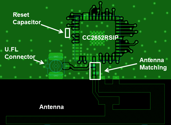
GUID-9A6F4CB7-7B9F-4C00-8151-53D8AD74A29F-low.png Figure 10-2 Module Layout Guidelines

Follow these RF layout recommendations for the CC2652RSIP module:

  • RF traces must have a chararcterisitc impedance of 50-Ω.
  • There must be no traces or ground under the antenna section.
  • RF traces must have via stitching on the ground plane beside the RF trace on both sides.
  • RF traces must be as short as possible.
  • The module must be as close to the PCB edge in consideration of the product enclosure and type of antenna being used.