ZHCSH09 October 2017 MSP432E401Y
PRODUCTION DATA.
- 1器件概述
- 2Revision History
- 3Device Characteristics
- 4Terminal Configuration and Functions
-
5Specifications
- 5.1 Absolute Maximum Ratings
- 5.2 ESD Ratings
- 5.3 Recommended Operating Conditions
- 5.4 Recommended DC Operating Conditions
- 5.5 Recommended GPIO Operating Characteristics
- 5.6 Recommended Fast GPIO Pad Operating Conditions
- 5.7 Recommended Slow GPIO Pad Operating Conditions
- 5.8 GPIO Current Restrictions
- 5.9 I/O Reliability
- 5.10 Current Consumption
- 5.11 Peripheral Current Consumption
- 5.12 LDO Regulator Characteristics
- 5.13 Power Dissipation
- 5.14 Thermal Resistance Characteristics, 128-Pin PDT (TQFP) Package
- 5.15
Timing and Switching Characteristics
- 5.15.1 Load Conditions
- 5.15.2 Power Supply Sequencing
- 5.15.3 Reset Timing
- 5.15.4
Clock Specifications
- 5.15.4.1 PLL Specifications
- 5.15.4.2 PIOSC Specifications
- 5.15.4.3 Low-Frequency Oscillator Specifications
- 5.15.4.4 Hibernation Low-Frequency Oscillator Specifications
- 5.15.4.5 Main Oscillator Specifications
- 5.15.4.6 Main Oscillator Specification WIth ADC
- 5.15.4.7 System Clock Characteristics With USB Operation
- 5.15.5 Sleep Modes
- 5.15.6 Hibernation Module
- 5.15.7 Flash Memory
- 5.15.8 EEPROM
- 5.15.9 Input/Output Pin Characteristics
- 5.15.10 External Peripheral Interface (EPI)
- 5.15.11 Analog-to-Digital Converter (ADC)
- 5.15.12 Synchronous Serial Interface (SSI)
- 5.15.13 Inter-Integrated Circuit (I2C) Interface
- 5.15.14 Ethernet Controller
- 5.15.15 Universal Serial Bus (USB) Controller
- 5.15.16 Analog Comparator
- 5.15.17 Pulse-Width Modulator (PWM)
- 5.15.18 Emulation and Debug
-
6Detailed Description
- 6.1 Overview
- 6.2 Functional Block Diagram
- 6.3 Arm Cortex-M4F Processor Core
- 6.4 On-Chip Memory
- 6.5
Peripherals
- 6.5.1 External Peripheral Interface (EPI)
- 6.5.2 Cyclical Redundancy Check (CRC)
- 6.5.3 Advanced Encryption Standard (AES) Accelerator
- 6.5.4 Data Encryption Standard (DES) Accelerator
- 6.5.5 Secure Hash Algorithm/Message Digest Algorithm (SHA/MD5) Accelerator
- 6.5.6 Serial Communications Peripherals
- 6.5.7 System Integration
- 6.5.8 Advanced Motion Control
- 6.5.9 Analog
- 6.5.10 JTAG and Arm Serial Wire Debug
- 6.5.11 Peripheral Memory Map
- 6.6 Identification
- 6.7 Boot Modes
- 7Applications, Implementation, and Layout
- 8器件和文档支持
- 9机械、封装和可订购信息
Table 5-34 Electrical Characteristics for ADC at 2 Msps
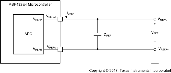
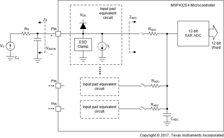
VREF+ = 3.3 V, fADC = 32 MHz, over operating free-air temperature (unless otherwise noted) (see Figure 5-26 and Figure 5-27)(1)| PARAMETER | MIN | TYP | MAX | UNIT | |
|---|---|---|---|---|---|
| Power supply requirements | |||||
| VDDA | ADC supply voltage | 2.97 | 3.3 | 3.63 | V |
| GNDA | ADC ground voltage | 0 | V | ||
| VDDA and GNDA voltage reference | |||||
| CREF | Voltage reference decoupling capacitance | 1.0 // 0.01 (2) | µF | ||
| External voltage reference input | |||||
| VREFA+ | Positive external voltage reference for ADC, when VREF field in the ADCCTL register is 0x1(3) | 2.4 | VDDA | VDDA | V |
| VREFA- | Negative external voltage reference for ADC, when VREF field in the ADCCTL register is 0x1 (3) | GNDA | GNDA | 0.3 | V |
| IVREF | Current on VREF+ input, using external VREF+ = 3.3 V | 330.5 | 440 | µA | |
| ILVREF | DC leakage current on VREF+ input when external VREF disabled | 2.0 | µA | ||
| CREF | External reference decoupling capacitance (3) | 1.0 // 0.01 (2) | µF | ||
| Analog input | |||||
| VADCIN | Single-ended, full-scale analog input voltage, internal reference(4)(5) | 0 | VDDA | V | |
| Differential, full-scale analog input voltage, internal reference (4)(6) | –VDDA | VVDDA | |||
| Single-ended, full-scale analog input voltage, external reference (3)(5) | VREFA- | VREFA+ | |||
| Differential, full-scale analog input voltage, external reference (3)(7) | –(VREFA+ – VREFA-) | VREFA+ – VREFA- | |||
| VINCM | Input common-mode voltage, differential mode (8) | [(VREFA+ + VREFA-) / 2] ±0.025 | V | ||
| IL | ADC input leakage current(9) | 2.0 | µA | ||
| RADC | ADC equivalent input resistance (9) | 2.5 | kΩ | ||
| CADC | ADC equivalent input capacitance (9) | 10 | pF | ||
| RS | Analog source resistance (9) | 250 | Ω | ||
| Sampling dynamics | |||||
| fADC | ADC conversion clock frequency(10) | 32 | MHz | ||
| fCONV | ADC conversion rate | 2 | Msps | ||
| tS | ADC sample time | 125 | ns | ||
| tC | ADC conversion time (11) | 0.5 | µs | ||
| tLT | Latency from trigger to start of conversion | 2 | ADC clock cycles | ||
| System performance when using external reference(12)(13) | |||||
| N | Resolution | 12 | bits | ||
| INL | Integral nonlinearity error, over full input range | ±1.5 | ±3.0 | LSB | |
| DNL | Differential nonlinearity error, over full input range | ±0.8 | +2.0/–1.0 (14) | LSB | |
| EO | Offset error | ±1.0 | ±3.0 | LSB | |
| EG | Gain error (15) | ±2.0 | ±3.0 | LSB | |
| ET | Total unadjusted error, over full input range (16) | ±2.5 | ±4.0 | LSB | |
| System performance when using internal reference | |||||
| N | Resolution | 12 | bits | ||
| INL | Integral nonlinearity error, over full input range | ±1.5 | ±3.0 | LSB | |
| DNL | Differential nonlinearity error, over full input range | ±0.8 | +2.0/–1.0 (14) | LSB | |
| EO | Offset error | ±5.0 | ±15.0 | LSB | |
| EG | Gain error (15) | ±10.0 | ±30.0 | LSB | |
| ET | Total unadjusted error, over full input range (16) | ±10.0 | ±30.0 | LSB | |
| Dynamic characteristics(17)(18) | |||||
| SNRD | Signal-to-noise-ratio, differential input, VADCIN: –20 dB FS, 1 kHz (19) | 68 | 72 | dB | |
| SDRD | Signal-to-distortion ratio, differential input, VADCIN: –3 dB FS, 1 kHz (19)(20)(21) | 70 | 75 | dB | |
| SNDRD | Signal-to-noise+distortion ratio, differential input, VADCIN: –3 dB FS, 1 kHz (19)(22)(23) | 65 | 70 | dB | |
| SNRS | Signal-to-noise-ratio, single-ended input, VADCIN: –20 dB FS, 1 kHz (24) | 58 | 65 | dB | |
| SDRS | Signal-to-distortion ratio, single-ended input, VADCIN: –3 dB FS, 1 kHz (20)(21) | 68 | 72 | dB | |
| SNDRS | Signal-to-noise+distortion ratio, single-ended input, VADCIN: –3 dB FS, 1 kHz (24)(22)(23) | 58 | 63 | dB | |
(1) Best design practices suggest placing static or quiet digital I/O signals adjacent to sensitive analog inputs to reduce capacitive coupling and crosstalk. Unexpected results can occur if a switching digital I/O is placed adjacent to an ADC input channel or voltage reference input. In addition, analog signals configured adjacent to ADC input channels or reference inputs must meet the RADC equivalent input resistance given in this table and must be band-limited to 100 kHz or lower.
(2) Two capacitors in parallel. These capacitors should be as close to the die as possible.
(3) Assumes external filtering network between VREFA+ and VREFA- as shown in Figure 5-26. External reference noise level must be under 12-bit (–74-dB) full scale input, over input bandwidth, measured at VREFA+ – VREFA-.
(4) Internal reference is connected directly between VDDA and VGNDA (VREFi = VDDA – VGNDA). In this mode, EO, EG, ET, and dynamic specifications are adversely affected due to internal voltage drop and noise on VDDA and GNDA. Internal reference voltage is selected when VREF field in the ADCCTL register is 0x0.
(5) VADCIN = VINP – VINN
(6) With signal common-mode voltage as VDDA / 2.
(7) With signal common-mode voltage as (VREF+ + VREF-) / 2.
(8) This parameter is defined as the average of the differential inputs.
(9) As shown in Figure 5-27, RADC is the total equivalent resistance in the input line all the way up to the sampling node at the input of the ADC.
(10) See Table 5-14 for full ADC clock frequency specification.
(11) ADC conversion time (tC) includes the ADC sample time (tS).
(12) A low-noise environment is assumed to obtain values close to specifications. The board must have good ground isolation between analog and digital grounds, a clean reference voltage is assumed, and input signal must be bandlimited to Nyquist bandwidth. No antialiasing filter is provided internally.
(13) ADC static measurements taken by averaging over several samples. At least 20-sample averaging is assumed to obtain expected typical or maximum specification values.
(14) 12-bit DNL
(15) Gain error is measured at maximum code after compensating for offset. Gain error is equivalent to"Full Scale Error." It can be given in % of slope error, or in LSB, as done here.
(16) Total Unadjusted Error is the maximum error at any one code versus the ideal ADC curve. It includes all other errors (offset error, gain error and INL) at any given ADC code.
(17) A low noise environment is assumed to obtain values close to spec. The board must have good ground isolation between analog and digital grounds and a clean reference voltage. The input signal must be band-limited to Nyquist bandwidth. No antialiasing filter is provided internally.
(18) ADC dynamic characteristics are measured using low-noise board design, with low-noise reference voltage (< –74 dB noise level in signal BW) and low-noise analog supply voltage. Board noise and ground bouncing couple into the ADC and affect dynamic characteristics. Clean external reference must be used to achieve the listed specifications.
(19) Differential signal with correct common-mode voltage, applied between two ADC inputs.
(20) SDR = –THD in dB.
(21) For higher-frequency inputs, expect degradation in SDR.
(22) SNDR = S/(N+D) = SINAD (in dB)
(23) Effective number of bits (ENOB) can be calculated from SNDR: ENOB = (SNDR – 1.76) / 6.02.
(24) Single-ended inputs are more sensitive to board and trace noise than differential inputs; SNR and SNDR measurements on single-ended inputs are highly dependent on how clean the test setup is. If the input signal is not well isolated on the board, higher noise than specified could be seen at the ADC output.
 Figure 5-26 ADC External Reference Filtering
 Figure 5-27 ADC Input Equivalency