ZHCSH09 October   2017 MSP432E401Y

PRODUCTION DATA.  

  1. 1器件概述
    1. 1.1 特性
    2. 1.2 应用
    3. 1.3 说明
    4. 1.4 功能框图
  2. 2Revision History
  3. 3Device Characteristics
    1. 3.1 Related Products
  4. 4Terminal Configuration and Functions
    1. 4.1 Pin Diagram
    2. 4.2 Pin Attributes
    3. 4.3 Signal Descriptions
      1. Table 4-3 Signal Descriptions
    4. 4.4 GPIO Pin Multiplexing
    5. 4.5 Buffer Type
    6. 4.6 Connections for Unused Pins
  5. 5Specifications
    1. 5.1  Absolute Maximum Ratings
    2. 5.2  ESD Ratings
    3. 5.3  Recommended Operating Conditions
    4. 5.4  Recommended DC Operating Conditions
    5. 5.5  Recommended GPIO Operating Characteristics
    6. 5.6  Recommended Fast GPIO Pad Operating Conditions
    7. 5.7  Recommended Slow GPIO Pad Operating Conditions
    8. 5.8  GPIO Current Restrictions
    9. 5.9  I/O Reliability
    10. 5.10 Current Consumption
    11. 5.11 Peripheral Current Consumption
    12. 5.12 LDO Regulator Characteristics
    13. 5.13 Power Dissipation
    14. 5.14 Thermal Resistance Characteristics, 128-Pin PDT (TQFP) Package
    15. 5.15 Timing and Switching Characteristics
      1. 5.15.1  Load Conditions
      2. 5.15.2  Power Supply Sequencing
        1. 5.15.2.1 Power and Brownout
          1. Table 5-3 Power and Brownout Levels
          2. 5.15.2.1.1 VDDA Levels
          3. 5.15.2.1.2 VDD Levels
          4. 5.15.2.1.3 VDDC Levels
          5. 5.15.2.1.4 VDD Glitch Response
          6. 5.15.2.1.5 VDD Droop Response
      3. 5.15.3  Reset Timing
        1. Table 5-4 Reset Characteristics
      4. 5.15.4  Clock Specifications
        1. 5.15.4.1 PLL Specifications
          1. Table 5-5 Phase Locked Loop (PLL) Characteristics
          2. 5.15.4.1.1 PLL Configuration
        2. 5.15.4.2 PIOSC Specifications
        3. 5.15.4.3 Low-Frequency Oscillator Specifications
          1. Table 5-9 Low-Frequency Oscillator Characteristics
        4. 5.15.4.4 Hibernation Low-Frequency Oscillator Specifications
          1. Table 5-10 Hibernation External Oscillator (XOSC) Input Characteristics
          2. Table 5-11 Hibernation Internal Low-Frequency Oscillator Clock Characteristics
        5. 5.15.4.5 Main Oscillator Specifications
          1. Table 5-12 Main Oscillator Input Characteristics
        6. 5.15.4.6 Main Oscillator Specification WIth ADC
          1. Table 5-14 System Clock Characteristics With ADC Operation
        7. 5.15.4.7 System Clock Characteristics With USB Operation
          1. Table 5-15 System Clock Characteristics With USB Operation
      5. 5.15.5  Sleep Modes
        1. Table 5-16 Wake From Sleep Characteristics
        2. Table 5-17 Wake From Deep Sleep Characteristics
      6. 5.15.6  Hibernation Module
        1. Table 5-18 Hibernation Module Battery Characteristics
        2. Table 5-19 Hibernation Module Characteristics
        3. Table 5-20 Hibernation Module Tamper I/O Characteristics
      7. 5.15.7  Flash Memory
        1. Table 5-21 Flash Memory Characteristics
      8. 5.15.8  EEPROM
        1. Table 5-22 EEPROM Characteristics
      9. 5.15.9  Input/Output Pin Characteristics
        1. Table 5-23 Fast GPIO Module Characteristics
        2. Table 5-24 Slow GPIO Module Characteristics
        3. 5.15.9.1    Types of I/O Pins and ESD Protection
          1. 5.15.9.1.1 Hibernate WAKE pin
            1. Table 5-25 Pad Voltage and Current Characteristics for Hibernate WAKE Pin
          2. 5.15.9.1.2 Nonpower I/O Pins
            1. Table 5-26 Nonpower I/O Pad Voltage and Current Characteristics
      10. 5.15.10 External Peripheral Interface (EPI)
        1. Table 5-28 EPI SDRAM Characteristics
        2. Table 5-29 EPI SDRAM Interface Characteristics
        3. Table 5-30 EPI Host-Bus 8 and Host-Bus 16 Interface Characteristics
        4. Table 5-31 EPI General-Purpose Interface Characteristics
        5. Table 5-32 EPI PSRAM Interface Characteristics
      11. 5.15.11 Analog-to-Digital Converter (ADC)
        1. Table 5-33 Electrical Characteristics for ADC at 1 Msps
        2. Table 5-34 Electrical Characteristics for ADC at 2 Msps
      12. 5.15.12 Synchronous Serial Interface (SSI)
        1. Table 5-35 SSI Characteristics
        2. Table 5-36 Bi- and Quad-SSI Characteristics
      13. 5.15.13 Inter-Integrated Circuit (I2C) Interface
        1. Table 5-37 I2C Characteristics
      14. 5.15.14 Ethernet Controller
        1. 5.15.14.1 DC Characteristics
          1. Table 5-38 Ethernet PHY DC Characteristics
        2. 5.15.14.2 Clock Characteristics for Ethernet
          1. Table 5-39 MOSC 25-MHz Crystal Specification
          2. Table 5-40 MOSC Single-Ended 25-MHz Oscillator Specification
        3. 5.15.14.3 AC Characteristics
          1. Table 5-41 Ethernet Controller Enable and Software Reset Timing
          2. Table 5-42 100Base-TX Transmit Timing
          3. Table 5-43 10Base-T Normal Link Pulse Timing
          4. Table 5-44 Auto-Negotiation Fast Link Pulse (FLP) Timing
          5. Table 5-45 100Base-TX Signal Detect Timing
      15. 5.15.15 Universal Serial Bus (USB) Controller
        1. Table 5-46 ULPI Interface Timing
      16. 5.15.16 Analog Comparator
        1. Table 5-47 Analog Comparator Characteristics
        2. Table 5-48 Analog Comparator Characteristics
        3. Table 5-49 Analog Comparator Voltage Reference Characteristics
        4. Table 5-50 Analog Comparator Voltage Reference Characteristics
      17. 5.15.17 Pulse-Width Modulator (PWM)
        1. Table 5-51 PWM Timing Characteristics
      18. 5.15.18 Emulation and Debug
        1. Table 5-52 JTAG Characteristics
  6. 6Detailed Description
    1. 6.1 Overview
    2. 6.2 Functional Block Diagram
    3. 6.3 Arm Cortex-M4F Processor Core
      1. 6.3.1 Processor Core
      2. 6.3.2 System Timer (SysTick)
      3. 6.3.3 Nested Vectored Interrupt Controller (NVIC)
      4. 6.3.4 System Control Block (SCB)
      5. 6.3.5 Memory Protection Unit (MPU)
      6. 6.3.6 Floating-Point Unit (FPU)
    4. 6.4 On-Chip Memory
      1. 6.4.1 SRAM
      2. 6.4.2 Flash Memory
      3. 6.4.3 ROM
      4. 6.4.4 EEPROM
      5. 6.4.5 Memory Map
    5. 6.5 Peripherals
      1. 6.5.1  External Peripheral Interface (EPI)
      2. 6.5.2  Cyclical Redundancy Check (CRC)
      3. 6.5.3  Advanced Encryption Standard (AES) Accelerator
      4. 6.5.4  Data Encryption Standard (DES) Accelerator
      5. 6.5.5  Secure Hash Algorithm/Message Digest Algorithm (SHA/MD5) Accelerator
      6. 6.5.6  Serial Communications Peripherals
        1. 6.5.6.1 Ethernet MAC and PHY
        2. 6.5.6.2 Controller Area Network (CAN)
        3. 6.5.6.3 Universal Serial Bus (USB)
        4. 6.5.6.4 Universal Asynchronous Receiver/Transmitter (UART)
        5. 6.5.6.5 Inter-Integrated Circuit (I2C)
        6. 6.5.6.6 Quad Synchronous Serial Interface (QSSI)
      7. 6.5.7  System Integration
        1. 6.5.7.1 Direct Memory Access (DMA)
        2. 6.5.7.2 System Control and Clocks
        3. 6.5.7.3 Programmable Timers
        4. 6.5.7.4 Capture Compare PWM (CCP) Pins
        5. 6.5.7.5 Hibernation (HIB) Module
        6. 6.5.7.6 Watchdog Timers
        7. 6.5.7.7 Programmable GPIOs
      8. 6.5.8  Advanced Motion Control
        1. 6.5.8.1 Pulse Width Modulation (PWM)
        2. 6.5.8.2 Quadrature Encoder With Index (QEI) Module
      9. 6.5.9  Analog
        1. 6.5.9.1 ADC
        2. 6.5.9.2 Analog Comparators
      10. 6.5.10 JTAG and Arm Serial Wire Debug
      11. 6.5.11 Peripheral Memory Map
    6. 6.6 Identification
    7. 6.7 Boot Modes
  7. 7Applications, Implementation, and Layout
    1. 7.1 System Design Guidelines
  8. 8器件和文档支持
    1. 8.1 入门和后续步骤
    2. 8.2 器件命名规则
    3. 8.3 工具和软件
    4. 8.4 文档支持
    5. 8.5 Community Resources
    6. 8.6 商标
    7. 8.7 静电放电警告
    8. 8.8 出口管制提示
    9. 8.9 术语表
  9. 9机械、封装和可订购信息

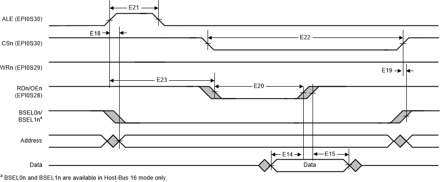
Table 5-30 EPI Host-Bus 8 and Host-Bus 16 Interface Characteristics

over operating free-air temperature (unless otherwise noted) (see Figure 5-19, Figure 5-20, Figure 5-21, and Figure 5-22)
NO.PARAMETERMINTYPMAXUNIT
E14 tISU Read data set up time 10 ns
E15 tIH Read data hold time 0 ns
E16 tDV WRn to write data valid 3.6 ns
E17 tDI Data hold from WRn invalid 1 EPI clock cycles
E18 tOV ALE/CSn to output valid 4 ns
E19 tOINV CSn to output invalid 4 ns
E20 tSTLOW WRn / RDn strobe duration low 1 EPI clock cycles
E21 tALEHIGH ALE duration high 1 EPI clock cycles
E22 tCSLOW CSn duration low 2 EPI clock cycles
E23 tALEST ALE rising to WRn / RDn strobe falling 2 EPI clock cycles
E24 tALEADD ALE falling to Address high impedance 1 EPI clock cycles
MSP432E401Y epi_hb_read.gifFigure 5-19 Host-Bus 8/16 Asynchronous Mode Read Timing
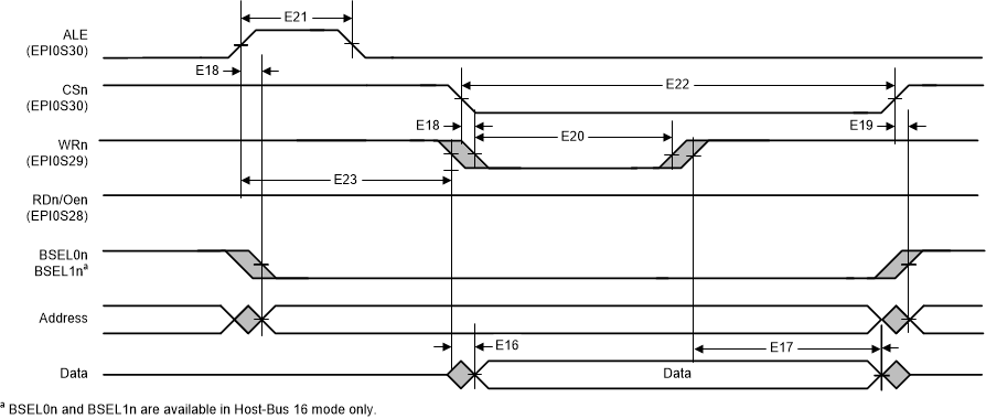
MSP432E401Y epi_hb_write.gifFigure 5-20 Host-Bus 8/16 Asynchronous Mode Write Timing
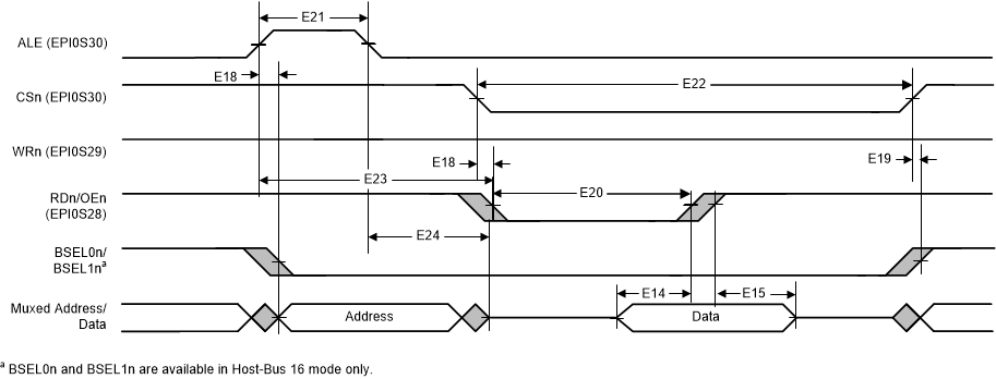
MSP432E401Y epi_hb_read_mux.gifFigure 5-21 Host-Bus 8/16 Mode Asynchronous Muxed Read Timing
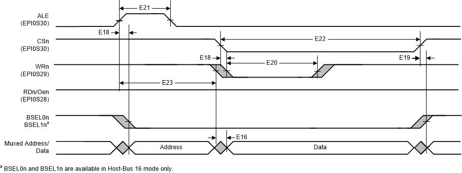
MSP432E401Y epi_hb_write_mux.gifFigure 5-22 Host-Bus 8/16 Mode Asynchronous Muxed Write Timing

Table 5-31 lists the switching characteristics of the general-purpose interface.