TIDT308 October   2022


  1.   Description
  2.   Features
  3.   Applications
  4. 1Test Prerequisites
    1. 1.1 Voltage and Current Requirements
    2. 1.2 Required Equipment
    3. 1.3 Considerations
    4. 1.4 Dimensions
    5. 1.5 Test Setup
  5. 2Testing and Results
    1. 2.1 Efficiency Graphs
    2. 2.2 Efficiency Data
    3. 2.3 Thermal Images
      1. 2.3.1 Top Side
      2. 2.3.2 Bottom Side
    4. 2.4 Bode Plots
  6. 3Waveforms
    1. 3.1 Switching
      1. 3.1.1 Secondary Side
      2. 3.1.2 Primary Side
        1. 3.1.2.1 Transistor Q8 Drain-Source
        2. 3.1.2.2 HS2-Pin of U1
          1. 3.1.2.2.1 Undershoot
          2. 3.1.2.2.2 Overshoot
    2. 3.2 Output Voltage Ripple
    3. 3.3 Load Transients
    4. 3.4 Start-Up Sequence
      1. 3.4.1 Full Load
      2. 3.4.2 Zero Load
      3. 3.4.3 Overload
    5. 3.5 Shutdown Sequence

Output Voltage Ripple

The output voltage ripple was measured by supplying the converter at 24 VDC and full load; the bandwidth limit of the scope was set to 20 MHz.
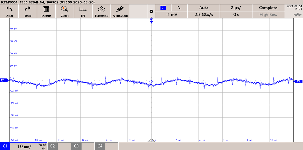
GUID-20220926-SS0I-XPMK-XLLQ-2BMF6ZRTN2HQ-low.png Figure 3-5 Output Voltage (10 mV/ div, 2 µs /div), AC Coupling, 20-MHz BWL)