TIDT308 October   2022


  1.   Description
  2.   Features
  3.   Applications
  4. 1Test Prerequisites
    1. 1.1 Voltage and Current Requirements
    2. 1.2 Required Equipment
    3. 1.3 Considerations
    4. 1.4 Dimensions
    5. 1.5 Test Setup
  5. 2Testing and Results
    1. 2.1 Efficiency Graphs
    2. 2.2 Efficiency Data
    3. 2.3 Thermal Images
      1. 2.3.1 Top Side
      2. 2.3.2 Bottom Side
    4. 2.4 Bode Plots
  6. 3Waveforms
    1. 3.1 Switching
      1. 3.1.1 Secondary Side
      2. 3.1.2 Primary Side
        1. 3.1.2.1 Transistor Q8 Drain-Source
        2. 3.1.2.2 HS2-Pin of U1
          1. 3.1.2.2.1 Undershoot
          2. 3.1.2.2.2 Overshoot
    2. 3.2 Output Voltage Ripple
    3. 3.3 Load Transients
    4. 3.4 Start-Up Sequence
      1. 3.4.1 Full Load
      2. 3.4.2 Zero Load
      3. 3.4.3 Overload
    5. 3.5 Shutdown Sequence

Overload

The following screen shots (Figure 3-9 and Figure 3-10) show the output voltage during start-up and overload protection, when the converter was loaded at 3.5 A.
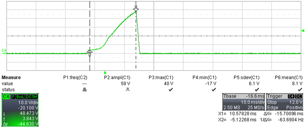
GUID-20220926-SS0I-LP22-WNL9-TCN7CBN1MHFS-low.pngFigure 3-9 Start-Up With Overload Condition (3.5 A), Time Base: 10 ms / div
  • Channel C4: Output voltage (10 V /div, 10 ms / div, DC coupling, 20-MHz BWL)

The same condition as in Figure 3-9 with different time base results in Figure 3-10.
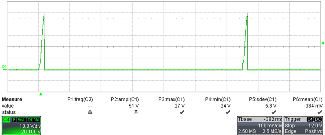
GUID-20220926-SS0I-3DJW-KQR0-C6CW1VCW6Z05-low.pngFigure 3-10 Start-Up With Overload Condition (3.5 A), Time Base: 100 ms / div
  • Channel C4: Output voltage (10 V / div, 100 ms / div, DC coupling, 20-MHz BWL)