TIDT308 October   2022
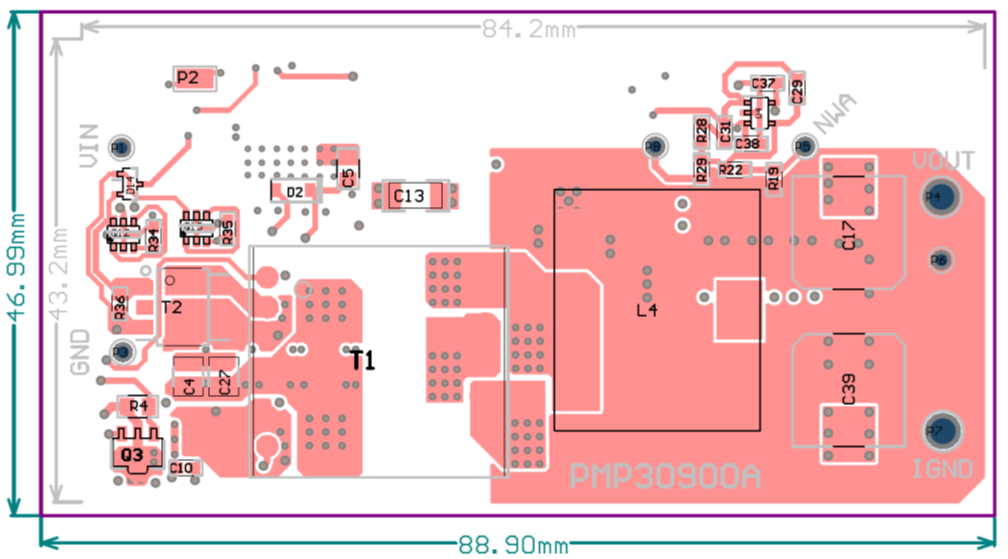
 

  1.   Description
  2.   Features
  3.   Applications
  4. 1Test Prerequisites
    1. 1.1 Voltage and Current Requirements
    2. 1.2 Required Equipment
    3. 1.3 Considerations
    4. 1.4 Dimensions
    5. 1.5 Test Setup
  5. 2Testing and Results
    1. 2.1 Efficiency Graphs
    2. 2.2 Efficiency Data
    3. 2.3 Thermal Images
      1. 2.3.1 Top Side
      2. 2.3.2 Bottom Side
    4. 2.4 Bode Plots
  6. 3Waveforms
    1. 3.1 Switching
      1. 3.1.1 Secondary Side
      2. 3.1.2 Primary Side
        1. 3.1.2.1 Transistor Q8 Drain-Source
        2. 3.1.2.2 HS2-Pin of U1
          1. 3.1.2.2.1 Undershoot
          2. 3.1.2.2.2 Overshoot
    2. 3.2 Output Voltage Ripple
    3. 3.3 Load Transients
    4. 3.4 Start-Up Sequence
      1. 3.4.1 Full Load
      2. 3.4.2 Zero Load
      3. 3.4.3 Overload
    5. 3.5 Shutdown Sequence

Dimensions

The board dimensions are 88.9 mm × 46.99 mm, with the height of 11.34 mm (Transformer T1), while the net PCB area dimensions are 84.22 mm x 43.2 mm.

The copper thickness of the six layer board is 70 µm on the outer layers and 35 µm on the inner layers (70-30-30-30-30-70).

GUID-20220926-SS0I-PG3F-K4QM-FCKHK7903RC8-low.png