TIDT260 March   2022


  1.   Description
  2.   Features
  3.   Applications
  4. 1Test Prerequisites
    1. 1.1 Voltage and Current Requirements
    2. 1.2 Considerations
    3. 1.3 Dimensions
  5. 2Testing and Results
    1. 2.1 Efficiency Graphs
    2. 2.2 Load Regulation
    3. 2.3 Line Regulation
    4. 2.4 Thermal Images
      1. 2.4.1 8-V Input Voltage
      2. 2.4.2 18-V Input Voltage
    5. 2.5 Bode Plots
  6. 3Waveforms
    1. 3.1 Switching
    2. 3.2 Output Voltage Ripple
    3. 3.3 Input Voltage Ripple
    4. 3.4 Load Transients
    5. 3.5 Start-Up Sequence
    6. 3.6 Shutdown Sequence
    7. 3.7 Spread Spectrum Feature

Input Voltage Ripple

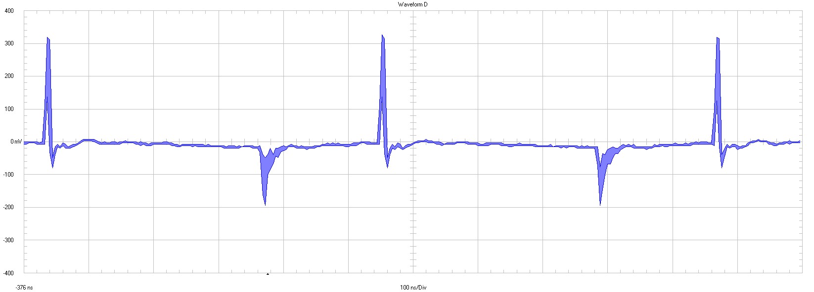
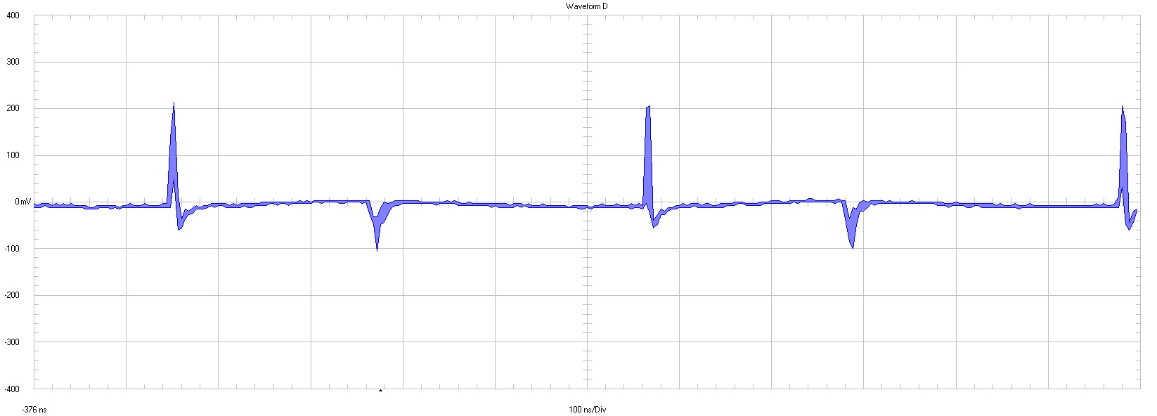
Input voltage ripple is shown in the following figures.
GUID-20220221-SS0I-110D-P0LJ-ZDN56NTHDMK3-low.jpg
100 mV / div, 100 ns / div, 20-MHz bandwidth
Figure 3-7 Input Voltage Ripple at 8-VIN
GUID-20220221-SS0I-KG7M-DMVC-5CTG3H96CXSF-low.jpg
100 mV / div, 100 ns / div, 20-MHz bandwidth
Figure 3-8 Input Voltage Ripple at 18-VIN