TIDT260 March 2022
3.7 Spread Spectrum Feature
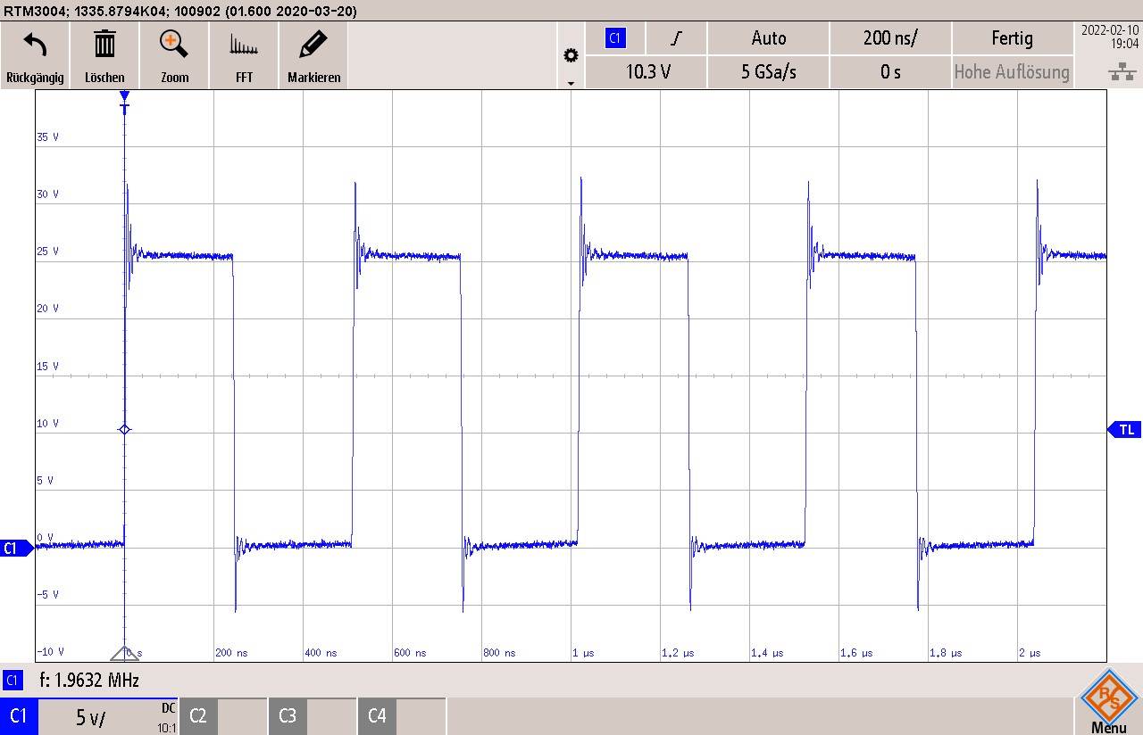
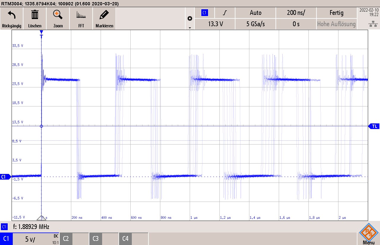
The spread spectrum features are demonstrated in the following figures.
 Figure 3-15 Disabled, MODE Tied to AGnd Using a
0-Ω Resistor
 Figure 3-16 Enabled, MODE Across R10 = 37.4-kΩ to
AGnd
Figure 3-16 Enabled, MODE Across R10 = 37.4-kΩ to
AGndDRSS, pseudo-dual random spread spectrum: low-frequency triangular switching frequency modulation, and triangular control voltage varies in its modulation frequency itself. In addition this control voltage is superimposed with a random noise, results in best noise reduction at switching frequency and closer harmonics as well as in the high RF range FM band and beyond.