TIDT260 March 2022
3.1 Switching
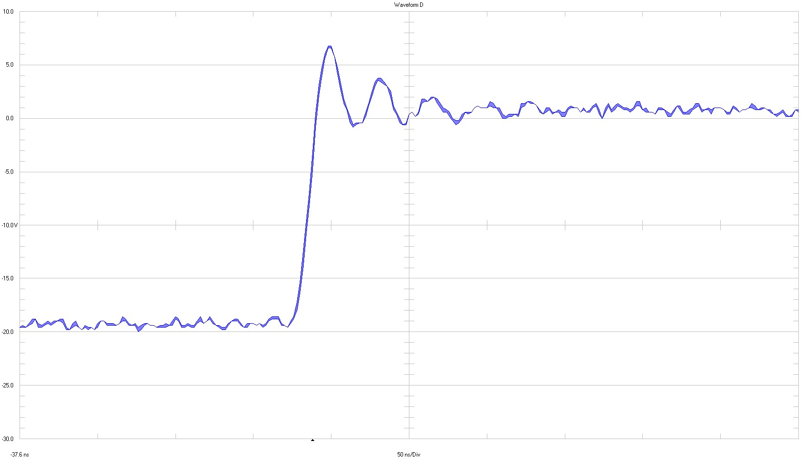
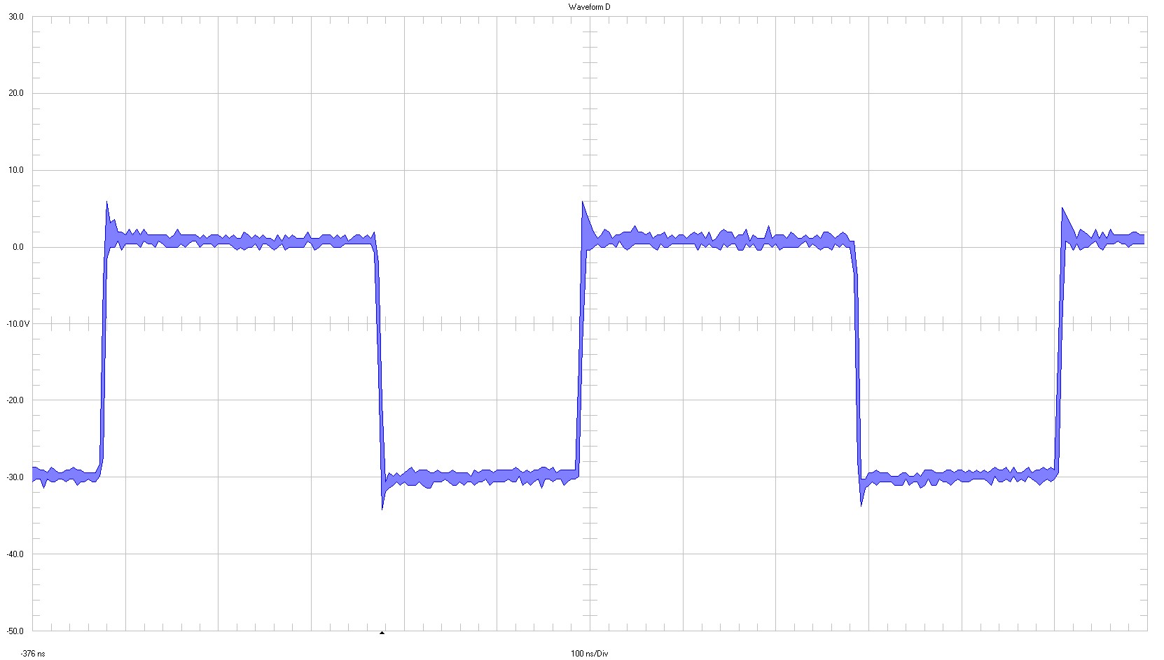
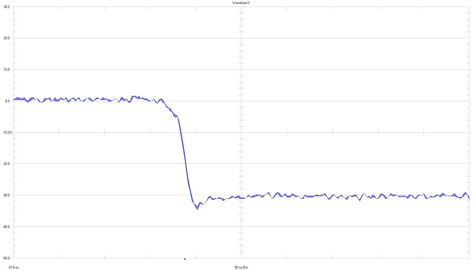
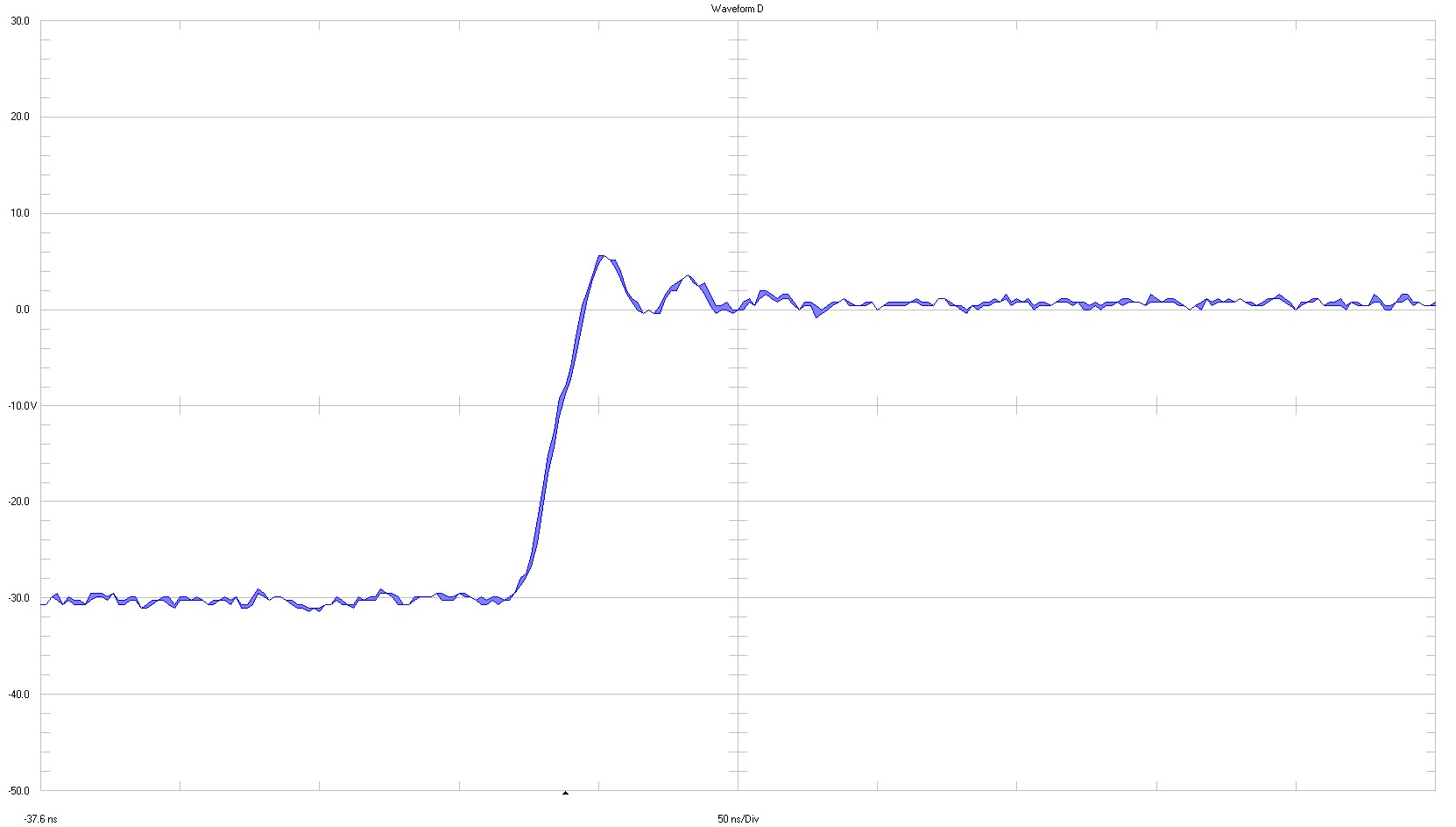
The switching waveforms are illustrated in the following images.
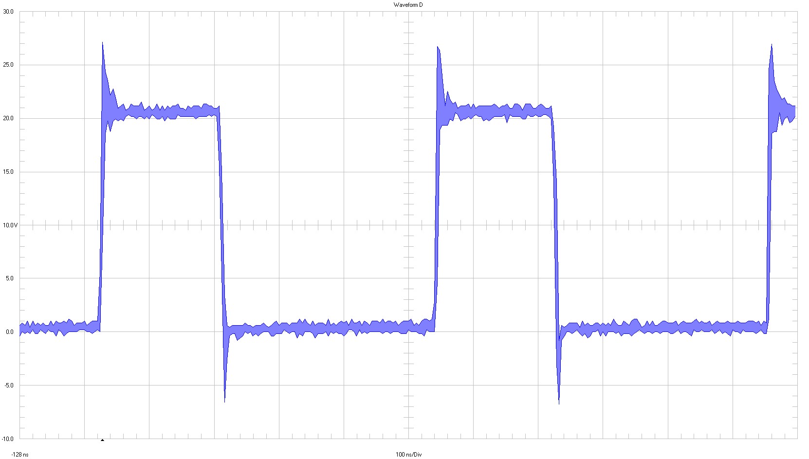
|
CH1 ⇒ 5-V / div, 100-ns / div, full bandwidth |
|
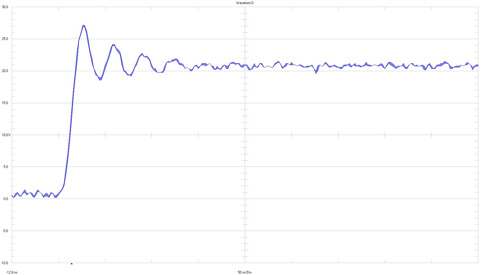
|
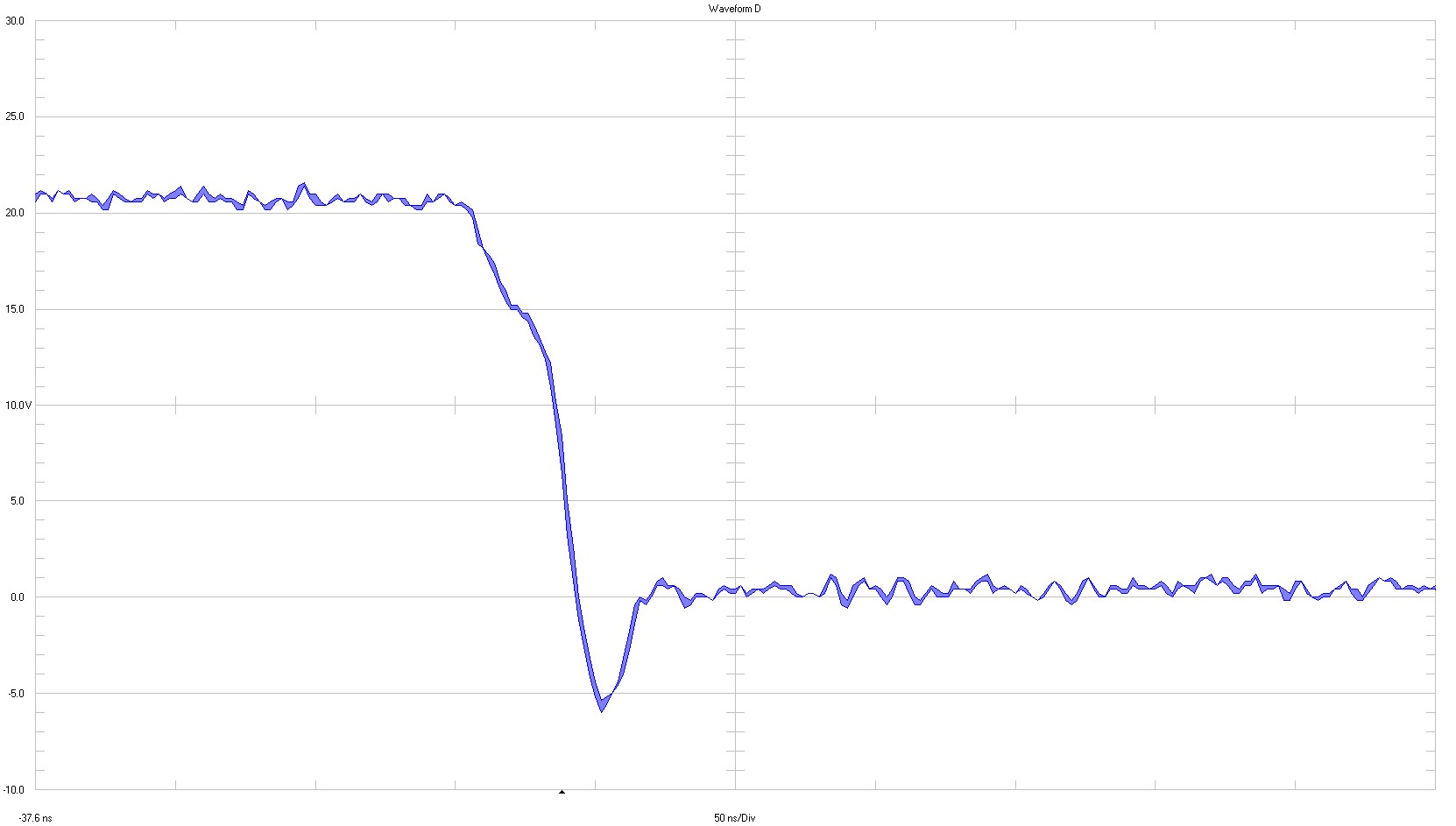
|
CH1 ⇒ 100-ns full scale |
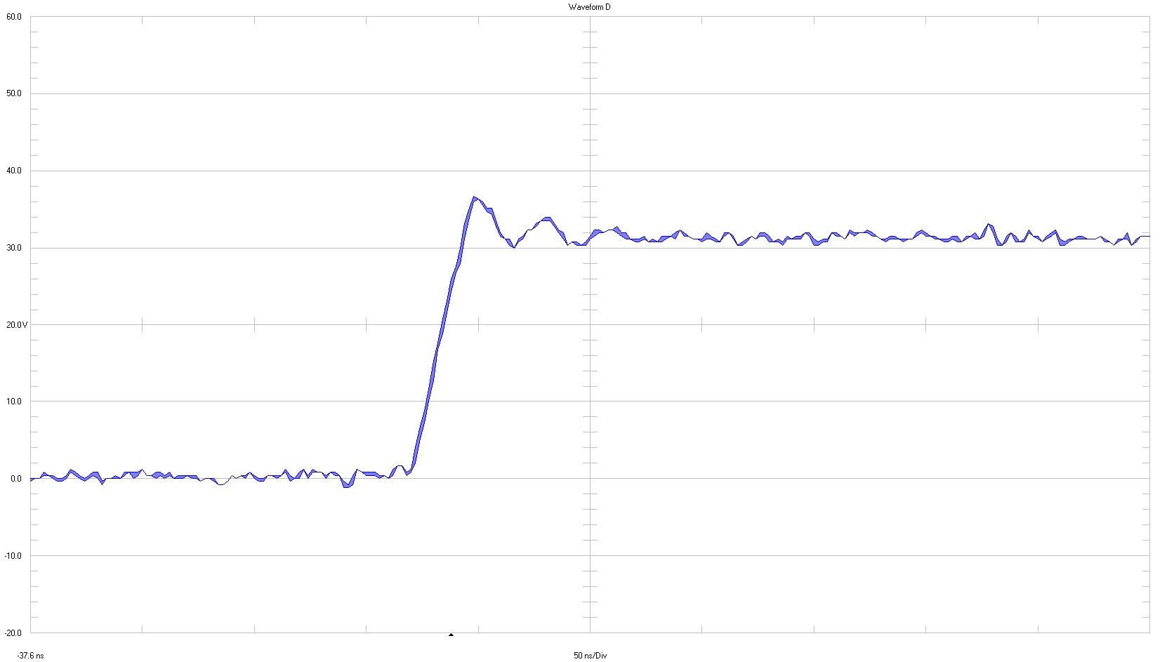
Figure 3-1 Switch Node (TP2 to GND), 8-V Input
Voltage
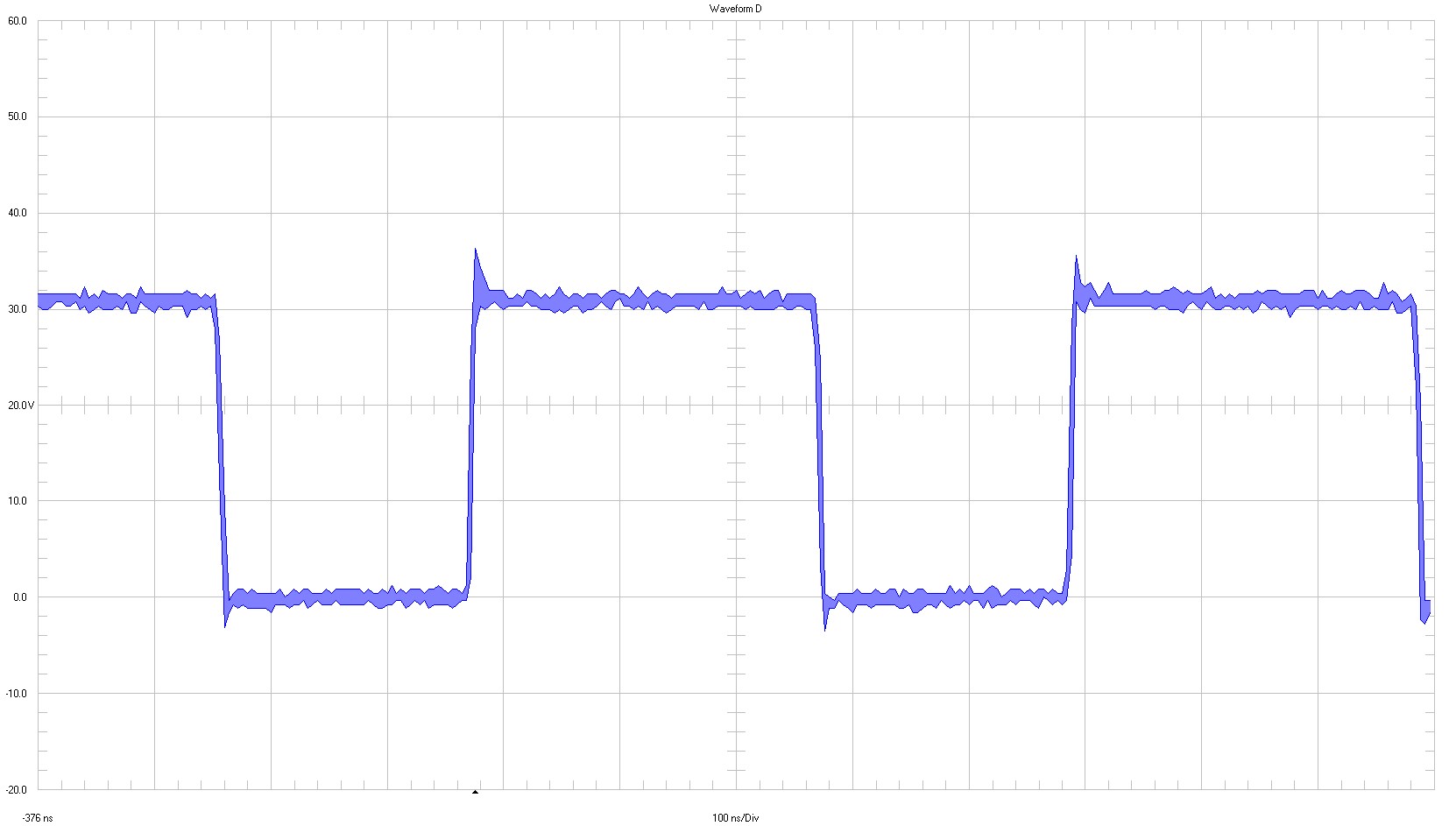
|
CH1 ⇒ 10 V / div 100-ns / div full bandwidth |
|
|
|
CH1 ⇒ 100-ns full scale |
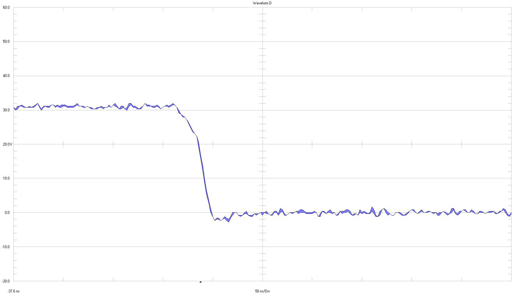
Figure 3-2 Switch Node (TP2 to GND), 18-V Input
Voltage
|
CH1 ⇒ 5 V / div 100 ns /div full bandwidth |
|
|
|
CH1 ⇒ 100-ns full scale |
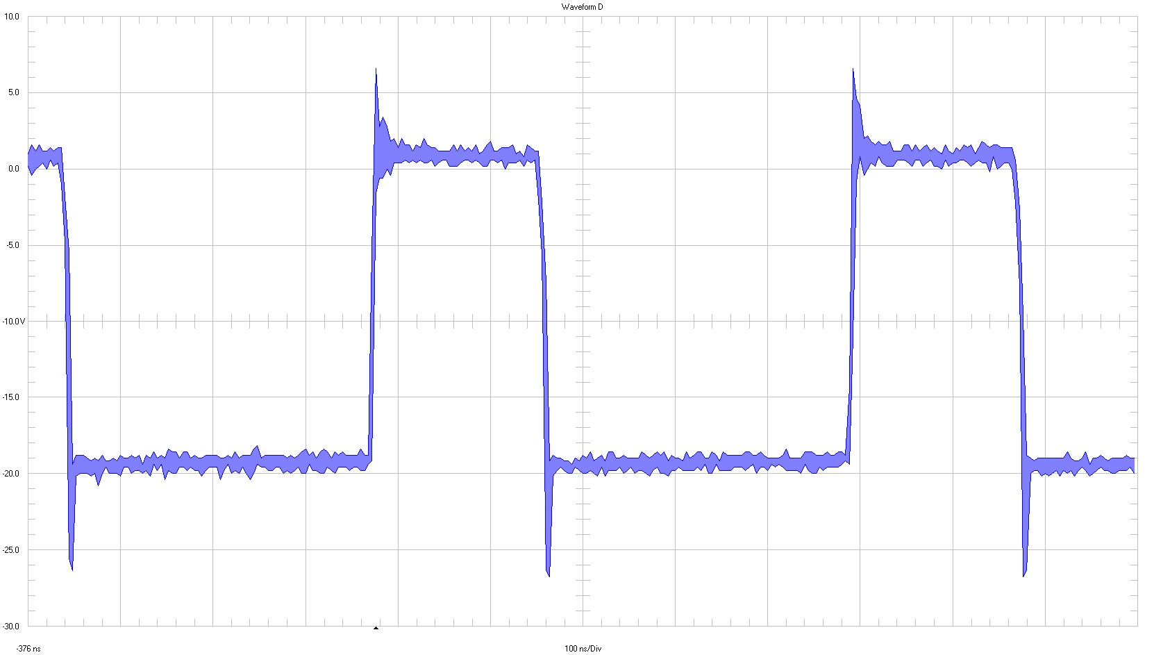
Figure 3-3 D1 to VOUT, 8-V Input
Voltage
|
CH1 ⇒ 10 V / div 100 ns /div full bandwidth |
|
|
|
CH1 ⇒ 100-ns full scale |
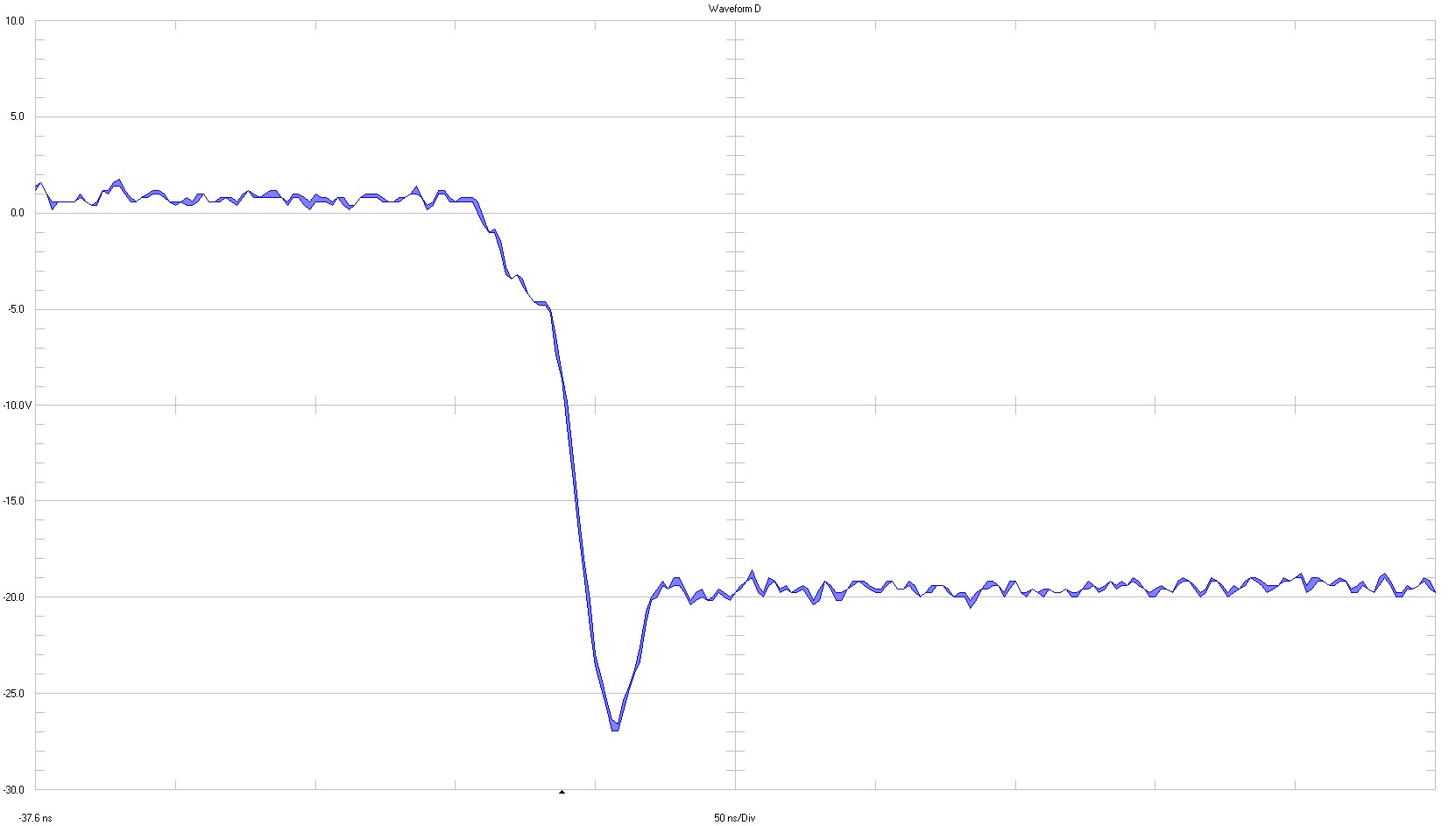
Figure 3-4 D1 to VOUT, 18-V Input
Voltage