TIDT195 September 2020 – MONTH
3.3 Output Voltage Ripple
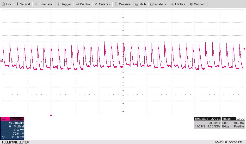
The output ripple voltage (AC coupled) is shown in the following image. The input voltage is 50 V and the 12-V output is loaded to 400 mA.
 Figure 3-14 Output Voltage Ripple (AC Coupled) (VOUT: 50 mV/div, 100 μs/div)
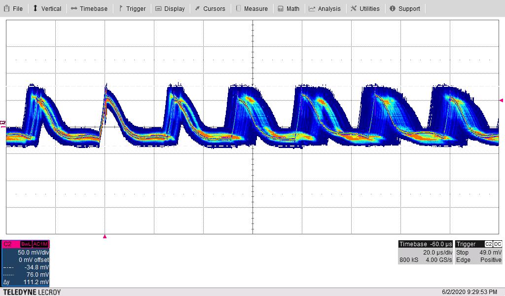
The output ripple voltage (AC coupled and scope persistence on) is shown in the following image. The input voltage is 50 V and the 12-V output is loaded to 400 mA. This shows the effects of frequency dithering and valley switching on the switch node waveform.
 Figure 3-15 Output Voltage Ripple (AC Coupled) (VOUT: 50 mV/div, 20 μs/div)
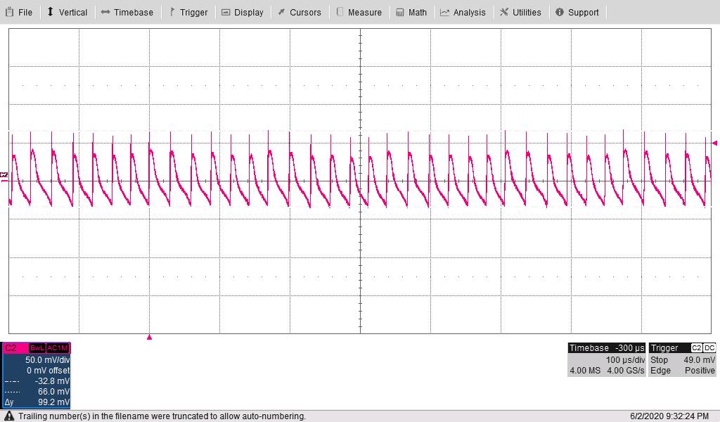
The output ripple voltage (AC coupled) is shown in the following image. The input voltage is 150 V and the 12-V output is loaded to 400 mA.
 Figure 3-16 Output Voltage Ripple (AC Coupled) (VOUT: 50 mV/div, 100 μs/div).