TIDT195 September 2020 – MONTH
3.4 Load Transients
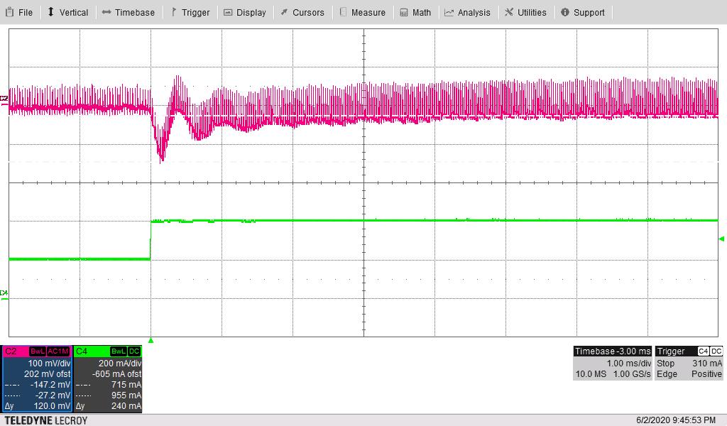
The following image shows the 12-V output voltage (AC coupled) when the load current is stepped between 200 mA and 400 mA (50% load step). VIN = 50 V.
 Figure 3-17 Load Transient, 12-V Output Voltage (AC
Coupled)
Figure 3-17 Load Transient, 12-V Output Voltage (AC
Coupled)(VOUT: 100 mV/div, IOUT: 200 mA/div, 1 ms/div)
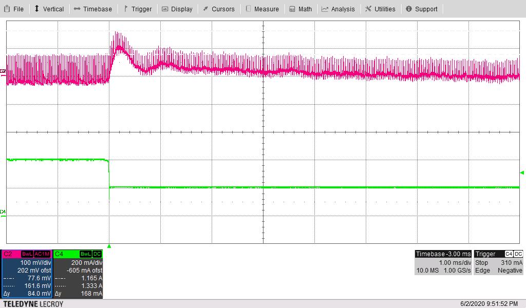
The following image shows the 12-V output voltage (AC coupled) when the load current is stepped between 400 mA and 200 mA (50% load step). VIN = 50 V.
 Figure 3-18 Load Transient, 12-V Output Voltage (AC
Coupled)
Figure 3-18 Load Transient, 12-V Output Voltage (AC
Coupled)(VOUT: 100 mV/div, IOUT: 200 mA/div, 1 ms/div)
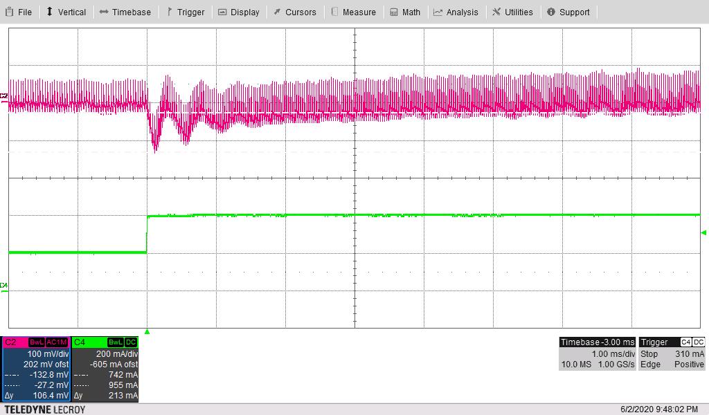
The following image shows the 12-V output voltage (AC coupled) when the load current is stepped between 200 mA and 400 mA (50% load step). VIN = 150 V.
 Figure 3-19 Load Transient, 12-V Output Voltage (AC
Coupled)
Figure 3-19 Load Transient, 12-V Output Voltage (AC
Coupled)(VOUT: 100 mV/div, IOUT: 200 mA/div, 1 ms/div).
 Figure 3-20 Load Transient, 12-V Output Voltage (AC
Coupled)
Figure 3-20 Load Transient, 12-V Output Voltage (AC
Coupled)(VOUT: 100 mV/div, IOUT: 200 mA/div, 1 ms/div).