TIDT195 September 2020 – MONTH
3.1 Start-up
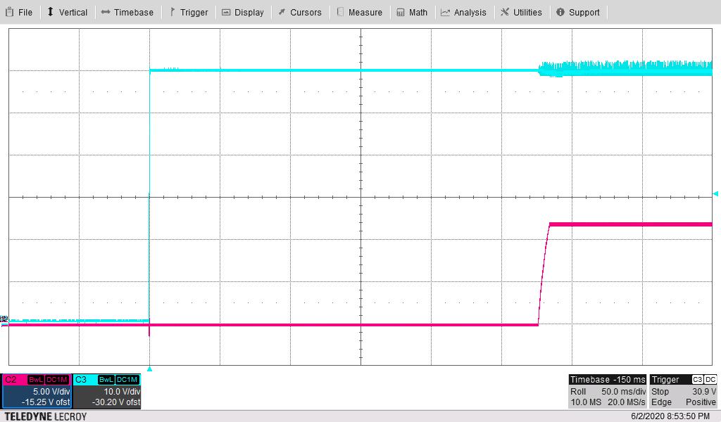
The following image shows the output voltage start-up waveform (RED) after the application of 60-V input (BLUE) with the 12-V output loaded to 400 mA.
 Figure 3-1 Output Voltage Start-up Waveform (VIN: 10 V/div, VOUT: 5 V/div, 50 ms/div)
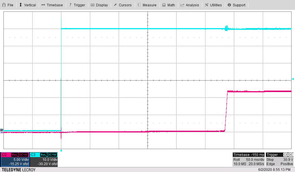
The following image shows the output voltage start-up waveform (RED) after the application of 60-V input (BLUE) with the 12-V output loaded to 0 mA.
 Figure 3-2 Output Voltage Start-up Waveform (VIN: 10 V/div, VOUT: 5 V/div, 50 ms/div)
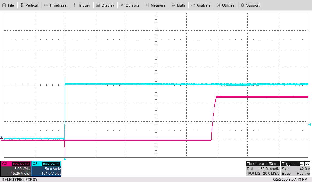
The following image shows the output voltage start-up waveform (RED) after the application of 150-V input (BLUE) with the 12-V output loaded to 400 mA.
 Figure 3-3 Output Voltage Start-up Waveform (VIN: 50 V/div, VOUT: 5V/div, 50 ms/div).
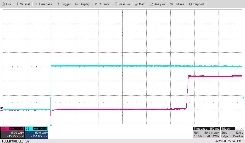
 The following image shows the output voltage start-up waveform (RED) after the application of 150-V input (BLUE) with the 12-V output loaded to 0 mA.
 Figure 3-4 Output Voltage Start-up Waveform (VIN: 50 V/div, VOUT: 5 V/div, 50 ms/div).