SPRZ272N September 2007 – April 2022 SM320F28335-EP , SM320F28335-HT , TMS320F28232 , TMS320F28232-Q1 , TMS320F28234 , TMS320F28234-Q1 , TMS320F28235 , TMS320F28235-Q1 , TMS320F28332 , TMS320F28333 , TMS320F28334 , TMS320F28335 , TMS320F28335-Q1
- 1Usage Notes and Advisories Matrices
- 2Nomenclature, Package Symbolization, and Revision Identification
-
3Silicon Revision A Usage Notes and
Advisories
- 3.1
Silicon Revision A Usage Notes
- 3.1.1 PIE: Spurious Nested Interrupt After Back-to-Back PIEACK Write and Manual CPU Interrupt Mask Clear Usage Note
- 3.1.2 Caution While Using Nested Interrupts
- 3.1.3 Watchdog: Watchdog Issues Reset After Bad Key is Written
- 3.1.4 McBSP: XRDY Bit can Hold the Not-Ready Status (0) if New Data is Written to the DX1 Register Without First Verifying if the XRDY Bit is in its Ready State (1)
- 3.1.5 Maximum Flash Program Time and Erase Time in Revision O of the TMS320F2833x, TMS320F2823x Real-Time Microcontrollers Data Sheet
- 3.2 Silicon Revision A Advisories
- 3.1
Silicon Revision A Usage Notes
- 4Silicon Revision 0 Usage Notes and Advisories
- 5Documentation Support
- 6Trademarks
- 7Revision History
Advisory
XINTF Rogue Write for Back-to-Back Accesses to x16/x32 Zones
Revision(s) Affected
0
Details
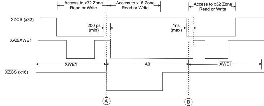
Figure 4-1 shows the behavior of zone chip select signals and XA0/ XWE1 for back-to-back accesses between zones configured for different data bus widths.
For the x32-bit zone (XTIMINGx[XSIZE] = 1) the A0/ XWE1 signal is the write enable XWE1. For the x16-bit zone (XTIMINGx[XSIZE] = 3) the A0/ XWE1 signal is address line A0.

When A0/ XWE1 changes functionality, the x32 zone chip select signal ( XZCS x32) changes state. Depending on the board design and peripherals attached to the XINTF, it is possible that an external memory or peripheral on the x32 zone may respond to A0/ XWE1 switching as a write access. If this happens, a rogue write to the x32 zone can occur.
Workaround(s)
- If all zones are configured for x16 operation, then no action is required.
- If all zones are configured for x32 operation, then XA0/
XWE1 will switch from XA0 to
XWE1 on the first access. After the first access, the XA0/
XWE1 pin will remain as
XWE1. To keep external devices from responding to the XA0/
XWE1 change, follow these steps when configuring the XINTF module:
- Enable the clock to the XINTF module.
- Configure the data-width and timing of the XINTF zones.
- Configure the zone chip select pins as GPIO inputs for the next step. This is the default behavior after reset.
- Perform a dummy read from a x32 XINTF zone. This read will force XA0/ XWE1 to behave as XWE1. Since the zone chip selects are configured as GPIO inputs, the external devices will not respond to XA0/ XWE1 switching to XWE1. After the first read, XA0/ XWE1 will continue to behave as XWE1.
- Configure the GPIO MUX registers for XINTF operation.
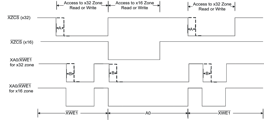
- Use external logic to delay the falling edge of the x32 zone chip select signal and the falling edge of the XWE1 signal as shown in Figure 4-2. With the delay the x32 zone chip select sees the XWE1 signal high at the critical points.
The timing configuration of the x32 zone must account for the additional delay. The zone chip select delay may require additional lead time. The XWE1 delay enable may require additional active write time. In addition, specify at least 1 trail cycle for writes to the x32 zone.

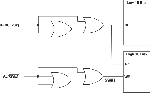
The delay can be created by using 74LVC32 quad OR gates or similar logic to create a delay line as shown in Figure 4-3.
 Figure 4-3 Example Delay Line Circuit
This has been fixed in Rev A silicon. The external delay logic is no longer required to avoid this issue in Rev A. The behavior of the XA0/ XWE1 signal has been modified such that it goes high during inactive cycles. Use the XBANK feature to force inactive cycles between back-to-back zone accesses. See the External Interface (XINTF) chapter of the TMS320x2833x, TMS320x2823x Real-Time Microcontrollers Technical Reference Manual for more information.