SPRUIM6A October 2018 – November 2020
- 1Introduction
- 2AM65x IDK Overview
-
3Common Processor Board
- 3.1 Key Features
- 3.2 Functional Block Diagram
- 3.3
Overview of Common Processor Board
- 3.3.1 Clocking
- 3.3.2 Reset
- 3.3.3 Power Requirements
- 3.3.4 Configuration
- 3.3.5 Memory Interfaces
- 3.3.6 Ethernet Interface
- 3.3.7 LCD Display Interface
- 3.3.8 USB 2.0 Interface
- 3.3.9 CSI-2 Interface
- 3.3.10 Application Card Interface
- 3.3.11 SERDES Interface
- 3.3.12 GPMC/DSS Interface
- 3.3.13 I2C Interface
- 3.3.14 SPI Interface
- 3.3.15 Timer and Interrupt
- 3.3.16 Fan Connector
- 4IDK Application Card
- 5x2 Lane PCIe Personality Card
-
6Known Issues
- 6.1 Determining the Revision and Date Code for the EVM
- 6.2 Known Issues for the A, E4, and E3 Revision
- 6.3 Known Issues for the E4 & E3 Revision
- 6.4
Known Issues for the E3 Revision
- 6.4.1 Resonance Observed on the SoC Side of Some Filters Associated with VDDA_1V8
- 6.4.2 Additional LDO Power Supply Needed for VDDA_1P8_SERDES0
- 6.4.3 Length of the RESET Signal to the PCIE Connectors on the SERDES Daughter Card
- 6.4.4 The PORz_OUT and MCU_PORz_OUT Signals Go High During Power Sequencing
- 6.4.5 Orientation of the Current Monitoring Shunt Resistors
- 6.4.6 SD Card IO Supply Capacitance
- 6.4.7 PHY Resistor Strapping Changed to Disable EEE Mode
- 6.4.8 The I2C Address for the I2C Boot Memory changed to 0x52
- 7Configuring the PRG0 and PRG1 Ethernet Interface to MII
- 8Revision History
3.3.13 I2C Interface
There are five I2C interfaces on the common processor card. All the I2C interface signals use the 3.3-V I/O level.
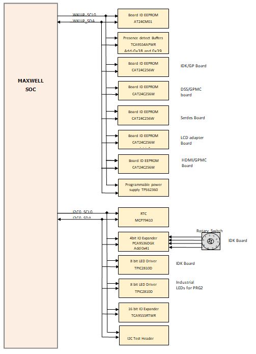
- WKUP_I2C0 is interfaced to a presence detect latch to identify the daughter cards which are presently installed. In addition, the processor board and each daughter card has a Board ID memory device connected to WKUP_I2C0. The Board ID memories contain identification and configuration information for the cards. The WKUP_I2C0 is also used to communicate with the power supply IC for the SoC_MPU rail, allowing modification of the voltage.
- I2C0 is connected to the on-card RTC, LED driver, I/O expander, and application connector to interface the I/O expander. This I2C is also connected to a test header J33 for AM65x processor slave operation. Pin outs of the I2C test header is given in Table 3-33.
Table 3-33 I2C Test Header (J33) Pin-out
Pin no. Signal 1 DGND 2 I2C0_SDA 3 I2C0_SCL - I2C1 is connected to a display adapter connector.
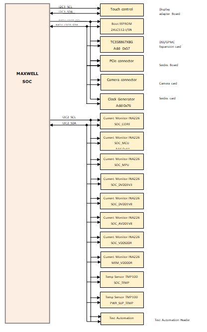
- MCU_I2C0 is connected to BOOT EEPROM, SERDES connector, GPMC/DSS connector, display port adopter interface, and camera connector.
- I2C2 is connected to current monitors, temperature sensors, and the test automation header.
I2C0 and I2C1 are powered by VDDSHV_GENERAL, WKUP_I2C0 and MCU_I2C0 are powered by VDDS_WKUP_GENERAL, and I2C2 is powered by VDDSHV_GPMC supply.
One test header for I2C0 is provided for any external validation. Figure 3-22 and Figure 3-23 depicts the I2C tree.
 Figure 3-22 I2C Interfaces and Address Assignment to its Peripherals (1 of 2)
 Figure 3-23 I2C Interfaces and Address Assignment to its Peripherals (2 of 2)