SPRUIM6A October 2018 – November 2020
- 1Introduction
- 2AM65x IDK Overview
-
3Common Processor Board
- 3.1 Key Features
- 3.2 Functional Block Diagram
- 3.3
Overview of Common Processor Board
- 3.3.1 Clocking
- 3.3.2 Reset
- 3.3.3 Power Requirements
- 3.3.4 Configuration
- 3.3.5 Memory Interfaces
- 3.3.6 Ethernet Interface
- 3.3.7 LCD Display Interface
- 3.3.8 USB 2.0 Interface
- 3.3.9 CSI-2 Interface
- 3.3.10 Application Card Interface
- 3.3.11 SERDES Interface
- 3.3.12 GPMC/DSS Interface
- 3.3.13 I2C Interface
- 3.3.14 SPI Interface
- 3.3.15 Timer and Interrupt
- 3.3.16 Fan Connector
- 4IDK Application Card
- 5x2 Lane PCIe Personality Card
-
6Known Issues
- 6.1 Determining the Revision and Date Code for the EVM
- 6.2 Known Issues for the A, E4, and E3 Revision
- 6.3 Known Issues for the E4 & E3 Revision
- 6.4
Known Issues for the E3 Revision
- 6.4.1 Resonance Observed on the SoC Side of Some Filters Associated with VDDA_1V8
- 6.4.2 Additional LDO Power Supply Needed for VDDA_1P8_SERDES0
- 6.4.3 Length of the RESET Signal to the PCIE Connectors on the SERDES Daughter Card
- 6.4.4 The PORz_OUT and MCU_PORz_OUT Signals Go High During Power Sequencing
- 6.4.5 Orientation of the Current Monitoring Shunt Resistors
- 6.4.6 SD Card IO Supply Capacitance
- 6.4.7 PHY Resistor Strapping Changed to Disable EEE Mode
- 6.4.8 The I2C Address for the I2C Boot Memory changed to 0x52
- 7Configuring the PRG0 and PRG1 Ethernet Interface to MII
- 8Revision History
4.2.6 Ethernet Interface
Four RGMII/MII ports from the ICSSG domain of the AM65x processor are terminated to the application card connector. These ports in the IDK application board are connected to Gigabit Ethernet PHYs, and the output of the PHYs are terminated with RJ45 connectors (J1 and J3 stacked RJ45 connectors) with integrated magnetic.
All RJ45 ports support 1000 Mbps / 100 Mbps / 10 Mbps using RGMII, and 100 Mbps / 10 Mbps using MII.
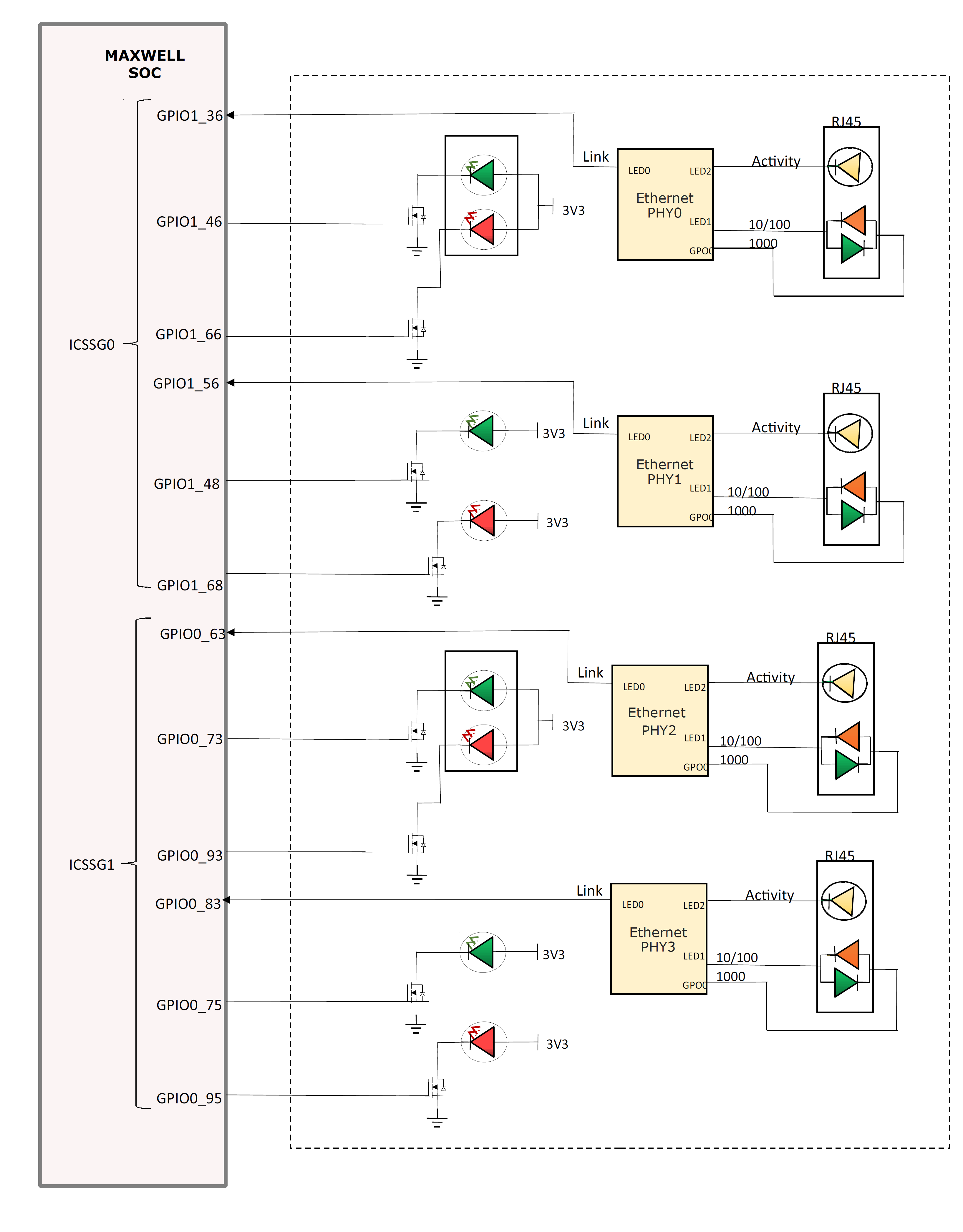
From the Ethernet PHY, LED1 and COL/GPIO are connected to dual LEDs of RJ45 to indicate 10/100 Mb or 1000-Mb link. The green LED indicates 10/100-Mb speed, and the orange LED indicates 1000-Mb speed.
LED2 is connected to RJ45 LED (Yellow) to indicate transmit/receive activity.
The IDK application board is delivered with all PHYs configured to operate in RGMII mode. Some industrial protocols require the use of the MII interface instead of RGMII. To change the interface to MII mode, modifications must be made, as shown in Table 4-6.
| PHY | Mount | Unmount |
|---|---|---|
| PHY 0 | R271 | R269 |
| R272 | R270 | |
| R274 | R273 | |
| R276 | R275 | |
| R278 | R277 | |
| R290 | R452 | |
| R444 | ||
| R445 | ||
| R453 | ||
| PHY 1 | R317 | R315 |
| R318 | R316 | |
| R320 | R319 | |
| R322 | R321 | |
| R324 | R323 | |
| R338 | R454 | |
| R446 | ||
| R447 | ||
| R455 | ||
| PHY 2 | R356 | R355 |
| R359 | R357 | |
| R361 | R358 | |
| R363 | R360 | |
| R364 | R362 | |
| R378 | R456 | |
| R448 | ||
| R449 | ||
| R457 | ||
| PHY 3 | R399 | R397 |
| R400 | R398 | |
| R403 | R401 | |
| R405 | R402 | |
| R406 | R404 | |
| R420 | R458 | |
| R450 | ||
| R451 | ||
| R459 |
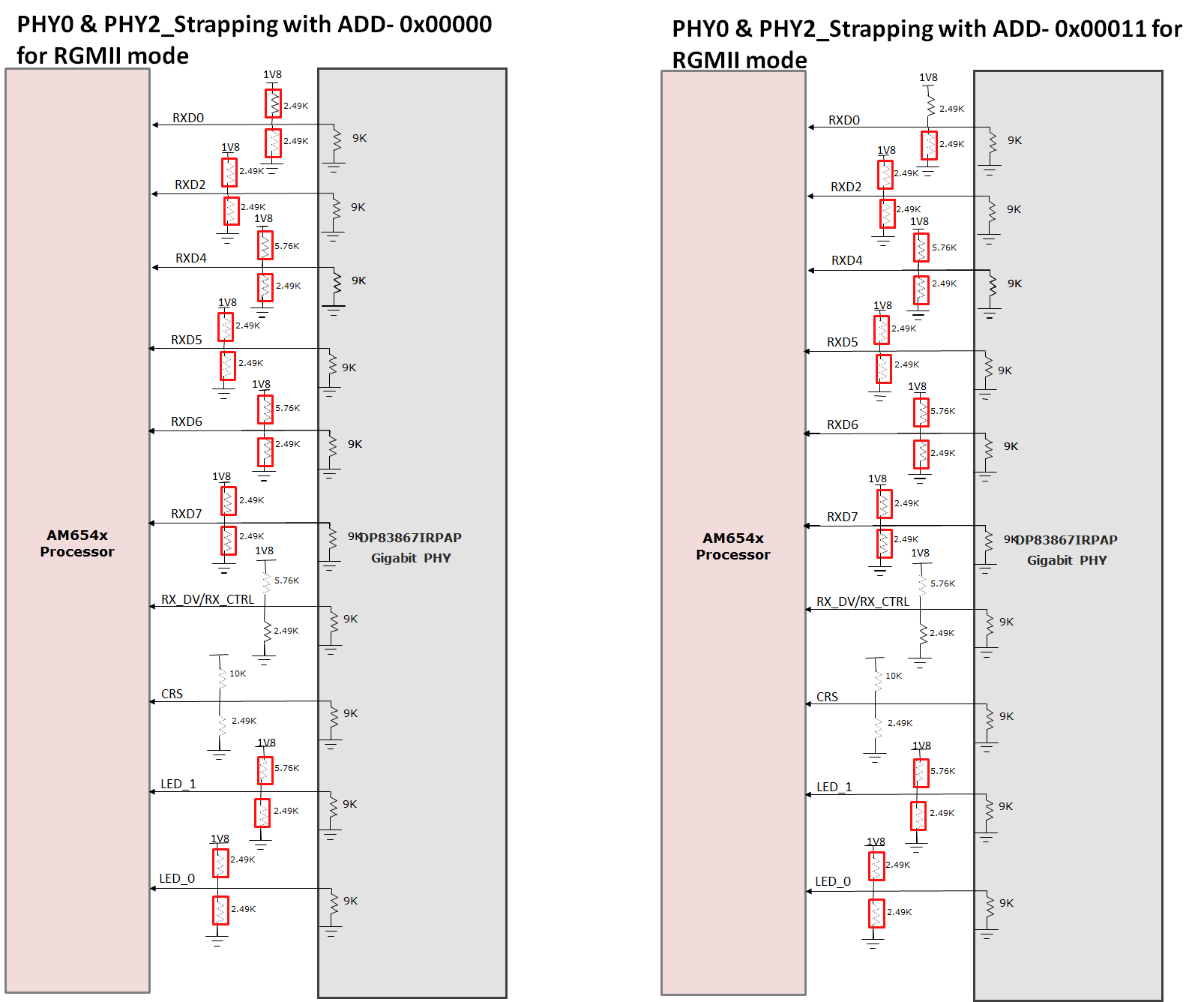
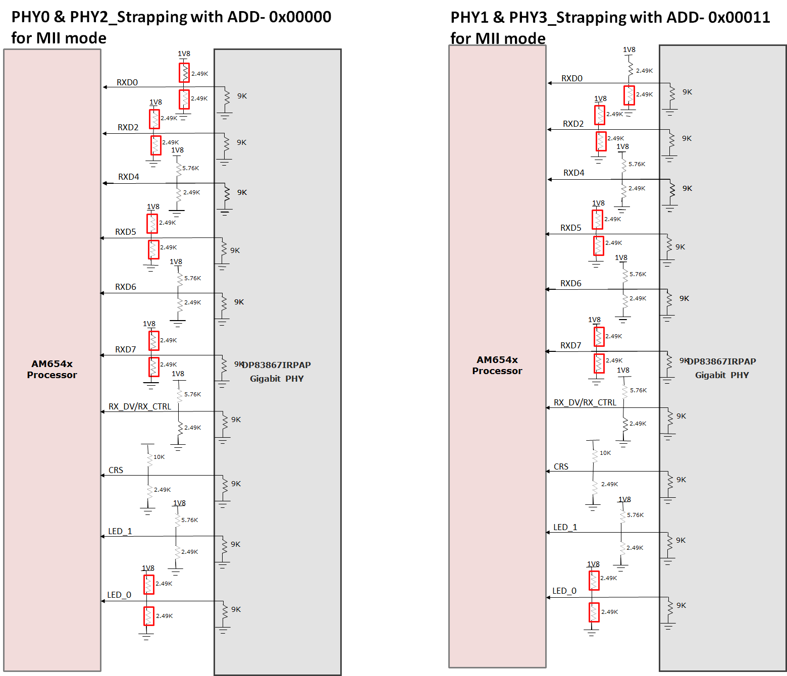
Default strapping details of all the PHYs are listed in Table 4-7.
| MII Mode Strap Setting | RGMII Mode Strap Setting | ||||||
|---|---|---|---|---|---|---|---|
| Signal | Mode | Pull Up | Pull Down | Mode | Pull Up | Pull Down | |
| PHY0 (J3A) (PHY Address-00000) | RX_D0 | 1 | Open | Open | 1 | Open | Open |
| RX_D2 | 1 | Open | Open | 1 | Open | Open | |
| RX_D4 | 3 | 5.76k | 2.49k | 1 | Open | Open | |
| RX_D5 | 1 | Open | Open | 1 | Open | Open | |
| RX_D6 | 3 | 5.76k | 2.49k | 1 | Open | Open | |
| RX_D7 | 1 | Open | Open | 1 | Open | Open | |
| RX_DV/RX_CTRL | 3 | 5.76k | 2.49k | 3 | 5.76k | 2.49k | |
| CRS | 2 | 10k | 2.49k | 2 | 10k | 2.49k | |
| LED_1 | 3 | 5.76k | 2.49k | 1 | Open | Open | |
| LED_0 | 1 | Open | Open | 1 | Open | Open | |
| PHY1 (J3B) (PHY Address-00011) | RX_D0 | 4 | 2.49K | Open | 4 | 2.49K | Open |
| RX_D2 | 1 | Open | Open | 1 | Open | Open | |
| RX_D4 | 3 | 5.76k | 2.49k | 1 | Open | Open | |
| RX_D5 | 1 | Open | Open | 1 | Open | Open | |
| RX_D6 | 3 | 5.76k | 2.49k | 1 | Open | Open | |
| RX_D7 | 1 | Open | Open | 1 | Open | Open | |
| RX_DV/RX_CTRL | 3 | 5.76k | 2.49k | 3 | 5.76k | 2.49k | |
| CRS | 2 | 10k | 2.49k | 2 | 10k | 2.49k | |
| LED_1 | 3 | 5.76k | 2.49k | 1 | Open | Open | |
| LED_0 | 1 | Open | Open | 1 | Open | Open | |
| PHY2 (J1A) (PHY Address-00000) | RX_D0 | 1 | Open | Open | 1 | Open | Open |
| RX_D2 | 1 | Open | Open | 1 | Open | Open | |
| RX_D4 | 3 | 5.76k | 2.49k | 1 | Open | Open | |
| RX_D5 | 1 | Open | Open | 1 | Open | Open | |
| RX_D6 | 3 | 5.76k | 2.49k | 1 | Open | Open | |
| RX_D7 | 1 | Open | Open | 1 | Open | Open | |
| RX_DV/RX_CTRL | 3 | 5.76k | 2.49k | 3 | 5.76k | 2.49k | |
| CRS | 2 | 10k | 2.49k | 2 | 10k | 2.49k | |
| LED_1 | 3 | 5.76k | 2.49k | 1 | Open | Open | |
| LED_0 | 1 | Open | Open | 1 | Open | Open | |
| PHY3 (J1B) (PHY Address-00011) | RX_D0 | 4 | 2.49K | Open | 4 | 2.49K | Open |
| RX_D2 | 1 | Open | Open | 1 | Open | Open | |
| RX_D4 | 3 | 5.76k | 2.49k | 1 | Open | Open | |
| RX_D5 | 1 | Open | Open | 1 | Open | Open | |
| RX_D6 | 3 | 5.76k | 2.49k | 1 | Open | Open | |
| RX_D7 | 1 | Open | Open | 1 | Open | Open | |
| RX_DV/RX_CTRL | 3 | 5.76k | 2.49k | 3 | 5.76k | 2.49k | |
| CRS | 2 | 10k | 2.49k | 2 | 10k | 2.49k | |
| LED_1 | 3 | 5.76k | 2.49k | 1 | Open | Open | |
| LED_0 | 1 | Open | Open | 1 | Open | Open | |
 Figure 4-3 PRG0 and PRG1 Ethernet Strapping Diagram in RGMII Mode
 Figure 4-4 PRG0 and PRG1 Ethernet Strapping Diagram in MII Mode
Resistors marked with the red color box are DNI for those particular modes of operation.
Some of the GPIOs are used to indicate Ethernet activities, as shown in Figure 4-5.
 Figure 4-5 IDK Board Ethernet LEDs