SNVU754A October 2021 – November 2021 LM5013-Q1
3.2 Detailed Descriptions
This section describes the connectors and the test points on the EVM and how to properly connect, set up and use the LM5013-Q1EVM. See Figure 3-1 for a top view of the EVM.
- VOUTOutput voltage of the converter.
VOUT connector and test point connected to the power inductor and the output capacitors. Connect the loading device between VOUT and GND connectors to provide loading to the regulator. Connect the loading device to the board with short wires to handle the DC output current.
- GNDGround of the converter.
It is connected to the GND as well as the return terminals of the input and output capacitors. GND is the current return path for both supply voltage and load. Connect to supply and load grounds with short wires.
- VINInput voltage to the converter.
VIN connector and test point connects to the input capacitors and the VIN pin of the LM5013-Q1. Connect the supply voltage from a power supply or a battery between the VIN and GND connectors. The voltage range should be higher than 6 V for the device to be active. VVIN higher than 15-V provides a regulated 12-V output voltage. To avoid damaging the device VVIN should be no greater than 100-V. The current limit on the supply should be high enough to provide the needed supply current when the output is fully loaded. The supply voltage should be connected to the board with short wires. C7 is populated to avoid oscillation between the cable parasitic inductance and the low-ESR input ceramic capacitors.
- VIN-EMIInput voltage to input filter of the converter.
The supply voltage should be connected to the board with short wires.
The inductor/ferrite in series with input path have some DCR associated with them. Verifying datasheet specification should be done by shorting these components.
- GND-EMIGround connection near the input filter.
This is the current return path for the supply connected to VIN-EMI. It provides a direct connection to the input filter capacitors to filter conducted noise generated by the converter. Use VIN-EMI and GND-EMI connections at the input filter to minimize EMI.
- Input FilterEMI mitigation.
The input filter consists of a filter inductor, ferrite bead and ceramic capacitors. An electrolytic capacitor is included for bulk energy storage and input parallel damping.
- EN/UVLOTest point to monitor the EN/UVLO pin of the device.
This test point is to monitor the voltage on the device EN/UVLO pin.
- EN/UVLO Set EN/UVLO
By default, device is hard-enabled. Device enable/disable voltage would correspond to typical VEN-RISING and VEN-FALLING datasheet specification.
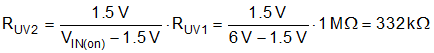
The enable/disable voltage can be varied by calculating for bottom UVLO resistor RUV2.
Calculate the lower UVLO resistor, RUV2 (R6), based on the desired turn-on voltage of 6 V and the selected upper UVLO resistor, RUV1 (R5) , of 1 MΩ using Equation 1.
- PGOODPGOOD
This flag indicates whether the output voltage has reached its regulation level. LM5013-Q1 PGOOD is an open-drain output that is tied to VOUT through pull-up resistor.