SLVUBX9 October   2020 TPS2640


  1.   Trademarks
  2. 1Introduction
    1. 1.1 EVM Features
    2. 1.2 EVM Applications
  3. 2Description
  4. 3Schematics
  5. 4General Configurations
    1. 4.1 Physical Access
    2. 4.2 Test Equipment
      1. 4.2.1 Power Supplies
      2. 4.2.2 Meters
      3. 4.2.3 Oscilloscope
      4. 4.2.4 Loads
    3. 4.3 Test Setup
    4. 4.4 Test Procedure
      1. 4.4.1 Preliminary Tests
      2. 4.4.2 Output Voltage Start-Up Time Test
      3. 4.4.3 Current Limit and Fault Responses Test
      4. 4.4.4 Output Short-Circuit Protection Test
      5. 4.4.5 Reverse Polarity Test
        1. 4.4.5.1 Overvoltage Clamp Response
  6. 5EVM Board Assembly Drawings and Layout Guidelines
    1. 5.1 PCB Drawings
  7. 6Bill Of Materials (BOM)

PCB Drawings

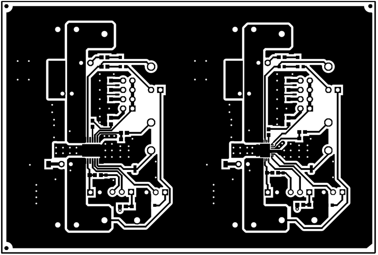
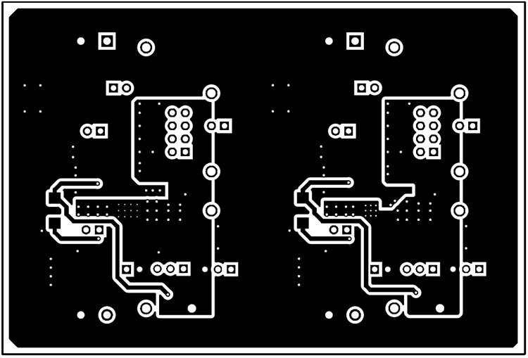
Figure 5-1 through Figure 5-3 show component placement and layout of the EVM.
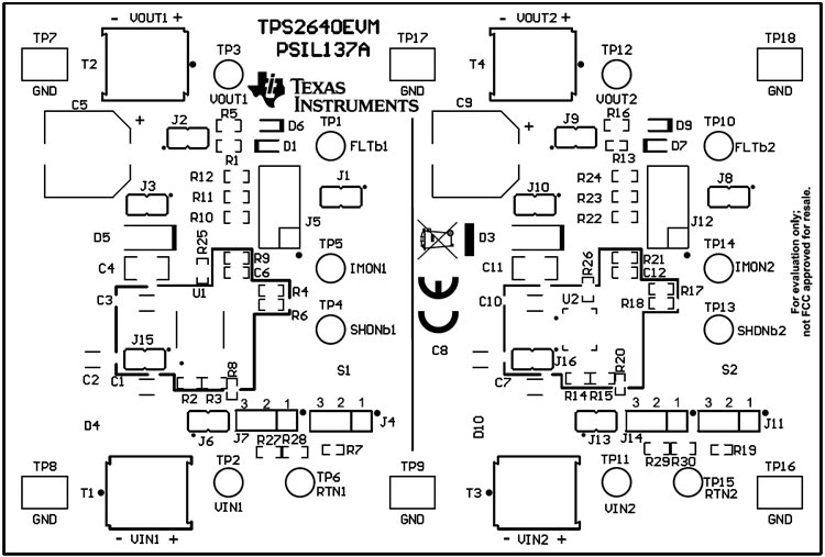
GUID-20200917-CA0I-2H21-P8JL-6THPRNXMBL1J-low.gifFigure 5-1 Top Side Placement.
GUID-20200917-CA0I-V99L-15FH-VNHSHHCJC4ZT-low.gifFigure 5-2 Top Layer.
GUID-20200917-CA0I-G6HS-RHZX-3NSJWGKZZQXB-low.gif Figure 5-3 Bottom Layer.